Datasheet 搜索 > 微控制器 > Microchip(微芯) > PIC12C671-04I/MF 数据手册 > PIC12C671-04I/MF 用户编程技术手册 1/14 页

¥ 14.956
PIC12C671-04I/MF 用户编程技术手册 - Microchip(微芯)
制造商:
Microchip(微芯)
分类:
微控制器
封装:
DFN-8
描述:
EPROM存储器编程规范 EPROM Memory Programming Specification
Pictures:
3D模型
符号图
焊盘图
引脚图
产品图
页面导航:
引脚图在P1Hot
电气规格在P11
导航目录
PIC12C671-04I/MF数据手册
Page:
of 14 Go
若手册格式错乱,请下载阅览PDF原文件
2001 Microchip Technology Inc. DS40175C-page 1
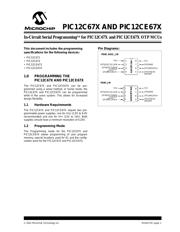
PIC12C67X AND PIC12CE67X
This document includes the programming
specifications for the following devices:
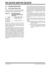
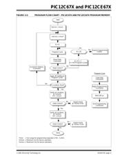
1.0 PROGRAMMING THE
PIC12C67X AND PIC12CE67X
The PIC12C67X and PIC12CE67X can be pro-
grammed using a serial method. In Serial mode, the
PIC12C67X and PIC12CE67X can be programmed
while in the users system. This allows for increased
design flexibility.
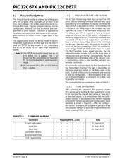
1.1 Hardware Requirements
The PIC12C67X and PIC12CE67X require two pro-
grammable power supplies, one for V
DD (2.0V to 6.0V
recommended) and one for V
PP (12V to 14V). Both
supplies should have a minimum resolution of 0.25V.
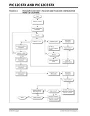
1.2 Programming Mode
The Programming mode for the PIC12C67X and
PIC12CE67X allows programming of user program
memory, special locations used for ID, and the config-
uration word for the PIC12C67X and PIC12CE67X.
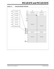
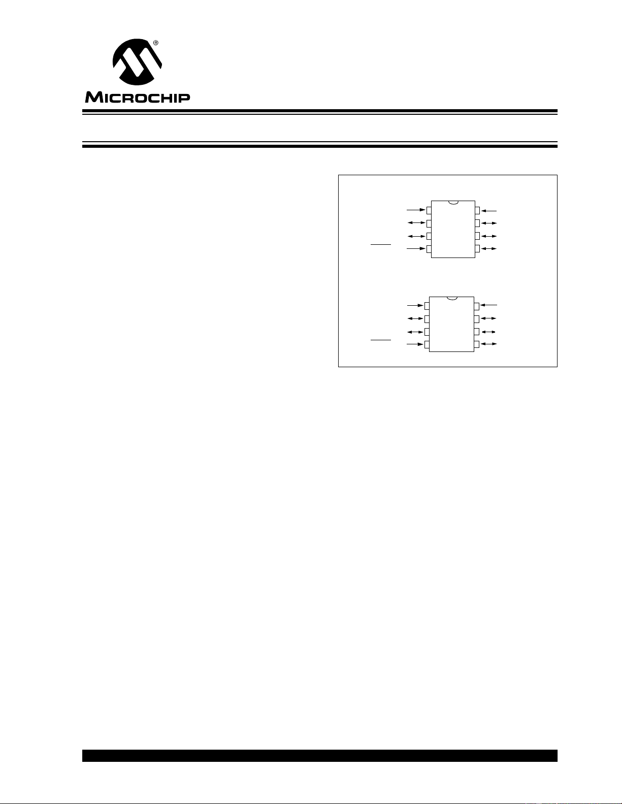
Pin Diagrams:
• PIC12C671
• PIC12C672
•PIC12CE673
•PIC12CE674
PDIP, SOIC, JW
8
7
6
5
1
2
3
4
PIC12C67X
GP5/OSC1/CLKIN
GP4/OSC2/AN3/
GP3/MCLR
/VPP
VDD
VSS
GP0/AN0
GP1/AN1/V
REF
GP2/T0CKI/
AN2/INT
CLKOUT
PDIP, JW
8
7
6
5
1
2
3
4
GP5/OSC1/CLKIN
GP4/OSC2/AN3/
GP3/MCLR
/VPP
VDD
VSS
GP0/AN0
GP1/AN1/V
REF
GP2/T0CKI/
AN2/INT
CLKOUT
PIC12CE67X
In-Circuit Serial Programming
TM
for PIC12C67X and PIC12CE67X OTP MCUs
器件 Datasheet 文档搜索
AiEMA 数据库涵盖高达 72,405,303 个元件的数据手册,每天更新 5,000 多个 PDF 文件
