Datasheet 搜索 > Microchip(微芯) > PIC12F1840T-E/SN 数据手册 > PIC12F1840T-E/SN 用户编程技术手册 2/38 页
 器件3D模型
¥ 13.359
PIC12F1840T-E/SN 用户编程技术手册 - Microchip(微芯)
制造商:
Microchip(微芯)
封装:
SOIC-8
描述:
PIC12F 系列 7 KB 闪存 256 B RAM 表面贴装 8 位 微控制器 - SOIC-8
Pictures:
3D模型
符号图
焊盘图
引脚图
产品图
页面导航:
引脚图在P2Hot
技术参数、封装参数在P30
电气规格在P30
导航目录
PIC12F1840T-E/SN数据手册
Page:
of 38 Go
若手册格式错乱,请下载阅览PDF原文件
PIC16F/LF1847/PIC12F/LF1840
DS41439A-page 2 Advanced Information 2010 Microchip Technology Inc.
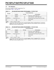
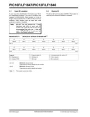
1.2 Pin Utilization
Five pins are needed for ICSP™ programming. The
pins are listed in Ta bl e 1- 1 and Table 1-2 .
TABLE 1-1: PIN DESCRIPTIONS DURING PROGRAMMING – PIC16F/LF1847
Pin Name
During Programming
Function Pin Type Pin Description
RB6 ICSPCLK I Clock Input – Schmitt Trigger Input
RB7 ICSPDAT I/O Data Input/Output – Schmitt Trigger Input
RA5/MCLR
/VPP Program/Verify mode P
(1)
Program Mode Select/Programming Power Supply
V
DD VDD P Power Supply
V
SS VSS P Ground
Legend: I = Input, O = Output, P = Power
Note 1: In the PIC12F/LF1840 and
PIC16F/LF1847, the programming high voltage is internally generated. To activate the
Program/Verify mode, high voltage needs to be applied to MCLR
input. Since the MCLR is used for a level source,
MCLR
does not draw any significant current.
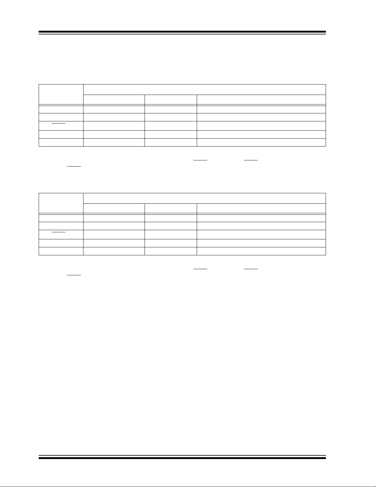
TABLE 1-2: PIN DESCRIPTIONS DURING PROGRAMMING – PIC12F/LF1840
Pin Name
During Programming
Function Pin Type Pin Description
RA1 ICSPCLK I Clock Input – Schmitt Trigger Input
RA0 ICSPDAT I/O Data Input/Output – Schmitt Trigger Input
RA3/MCLR
/VPP Program/Verify mode P
(1)
Program Mode Select/Programming Power Supply
V
DD VDD P Power Supply
V
SS VSS P Ground
Legend: I = Input, O = Output, P = Power
Note 1: In the PIC12F/LF1840
and PIC16F/LF1847, the programming high voltage is internally generated. To activate the
Program/Verify mode, high voltage needs to be applied to MCLR
input. Since the MCLR is used for a level source,
MCLR
does not draw any significant current.
器件 Datasheet 文档搜索
AiEMA 数据库涵盖高达 72,405,303 个元件的数据手册,每天更新 5,000 多个 PDF 文件
