Datasheet 搜索 > 8位微控制器 > Microchip(微芯) > PIC12F510-E/MS 数据手册 > PIC12F510-E/MS 用户编程技术手册 3/20 页
 器件3D模型
¥ 4.61
PIC12F510-E/MS 用户编程技术手册 - Microchip(微芯)
制造商:
Microchip(微芯)
分类:
8位微控制器
封装:
MSOP-8
描述:
PIC12F510 8 位闪存微控制器Microchip 的 PIC12 微控制器 (MCU) 是世界首个 8 引脚微控制器。 最初已经作为一次可编程 (OTP) 部件推出,此系列设备继续扩展为额外功能且添加了附加改进功能。 PIC12F510 系列微控制器基于 Microchip 的基线内核,带 2 层深硬件堆栈和 33 个指令。 这些 MCU 提供高达 2 MIPS、高达 1.5 K 字节程序内存和高达 38 字节 SRAM 数据内存。 板载可配置 RC 振荡器,精确度为 ±1%。### 特点33 个指令 2 级硬件堆栈 4 或 8 MHz 可选内部振荡器 6 个输入/输出引脚 一个比较器 一个 8 位计时器 4 通道 8 位模拟到数字转换器 (ADC) 在线串行编程 (ICSP) 在线调试 (ICD) ### PIC12F 微控制器### Microchip PIC12F 8 位 PIC® 微控制器Microchip 的 PIC12F 微控制器 (MCU) 是世界首个 8 引脚微控制器。 最初已经作为一次可编程 (OTP) 部件推出,此系列的设备将继续扩展为 Microchip 添加额外功能,进一步提高规格,并继续提供比以前更大的值。 PIC12F 成功的关键是在一个 8 引脚封装中允许六个输入/输出通道的内部 RC 振荡器。 此 RC 振荡器的更高版本可在 31kHz 和 32MHz 之间配置。展开
Pictures:
3D模型
符号图
焊盘图
引脚图
产品图
页面导航:
引脚图在P1Hot
电气规格在P17
导航目录
PIC12F510-E/MS数据手册
Page:
of 20 Go
若手册格式错乱,请下载阅览PDF原文件

© 2007 Microchip Technology Inc. DS41257B-page 3
PIC12F510
3.0 COMMANDS AND
ALGORITHMS
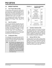
3.1 Program/Verify Mode
The Program/Verify mode is entered by holding pins
ICSPCLK and ICSPDAT low while raising V
DD pin from
V
IL to VDD. Then raise VPP from VIL to VIHH. Once in
this mode, the user program memory and configuration
memory can be accessed and programmed in serial
fashion. Clock and data are Schmitt Trigger input in this
mode.
The sequence that enters the device into the Program-
ming/Verify mode places all other logic into the Reset
state (the MCLR
pin was initially at VIL). This means
that all I/O are in the Reset state (high-impedance
inputs).
3.1.1 PROGRAMMING
The programming sequence loads a word, programs,
verifies and finally increments the PC.
Program/Verify mode entry will set the address to
0x7FF. The Increment Address command will
increment the PC. The available commands are shown
in Table 3-1.
FIGURE 3-1: ENTERING HIGH
VOLTAGE PROGRAM/
VERIFY MODE
3.1.2 SERIAL PROGRAM/VERIFY
OPERATION
The ICSPCLK pin is used for clock input and the
ICSPDAT pin is used for data input/output during serial
operation. To input a command, the clock pin is cycled
six times. Each command bit is latched on the falling
edge of the clock with the LSb of the command being
input first. The data must adhere to the setup (T
SET1)
and hold (T
HLD1) times with respect to the falling edge
of the clock (see Table 6-1).
Commands that do not have data associated with them
are required to wait a minimum of T
DLY2 measured
from the falling edge of the last command clock to the
rising edge of the next command clock (see Table 6-1).
Commands that do have data associated with them
(Read and Load) are also required to wait TDLY2
between the command and the data segment
measured from the falling edge of the last command
clock to the rising edge of the first data clock. The data
segment, consisting of 16 clock cycles, can begin after
this delay.
The first and last clock pulses during the data segment
correspond to the Start and Stop bits, respectively.
Input data is a “don’t care” during the Start and Stop
cycles. The 14 clock pulses between the Start and Stop
cycles clock the 14 bits of input/output data. Data is
transferred LSb first.
During Read commands, in which the data is output
from the PIC12F510, the ICSPDAT pin transitions from
the high-impedance input state to the low-impedance
output state at the rising edge of the second data clock
(first clock edge after the Start cycle). The ICSPDAT pin
returns to the high-impedance state at the rising edge
of the 16th data clock (first edge of the Stop cycle). See
Figure 3-3.
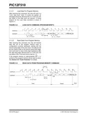
The commands that are available are described in
Table 3-1.
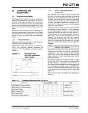
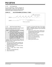
TABLE 3-1: COMMAND MAPPING FOR PIC12F510
VPP
THLD0
ICSPDAT
ICSPCLK
VDD
TPPDP
Note: After every End Programming command,
a delay of T
DIS is required.
Command Mapping (MSb … LSb) Data
Load Data for Program Memory xx00100, data (14), 0
Read Data from Program Memory xx01000, data (14), 0
Increment Address xx0110
Begin Programming xx1000Externally Timed
End Programming xx1110
Bulk Erase Program Memory xx1001Internally Timed
器件 Datasheet 文档搜索
AiEMA 数据库涵盖高达 72,405,303 个元件的数据手册,每天更新 5,000 多个 PDF 文件
