Datasheet 搜索 > 微控制器 > Microchip(微芯) > PIC12F510-I/P 数据手册 > PIC12F510-I/P 用户编程技术手册 1/20 页
 器件3D模型
¥ 4.927
PIC12F510-I/P 用户编程技术手册 - Microchip(微芯)
制造商:
Microchip(微芯)
分类:
微控制器
封装:
DIP-8
描述:
MICROCHIP PIC12F510-I/P 微控制器, 8位, 闪存, AEC-Q100, PIC12F5xx, 8 MHz, 1.5 KB, 38 Byte, 8 引脚, DIP
Pictures:
3D模型
符号图
焊盘图
引脚图
产品图
页面导航:
引脚图在P1Hot
电气规格在P17
导航目录
PIC12F510-I/P数据手册
Page:
of 20 Go
若手册格式错乱,请下载阅览PDF原文件
© 2007 Microchip Technology Inc. DS41257B-page 1
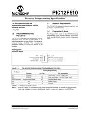
PIC12F510
This document includes the
programming specifications for the
following devices:
•PIC12F510
1.0 PROGRAMMING THE
PIC12F510
The PIC12F510 is programmed using a serial method.
The Serial mode will allow the PIC12F510 to be
programmed while in the user’s system. This allows for
increased design flexibility. This programming
specification applies to PIC12F510 devices in all
packages.
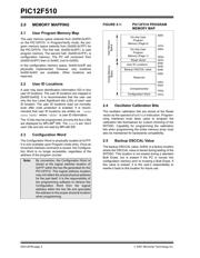
1.1 Hardware Requirements
The PIC12F510 requires one power supply for VDD
(5.0V) and one for VPP (12V).
1.2 Program/Verify Mode
The Program/Verify mode for the PIC12F510 allows
programming of user program memory, user ID loca-
tions, backup OSCCAL location and the Configuration
Word.
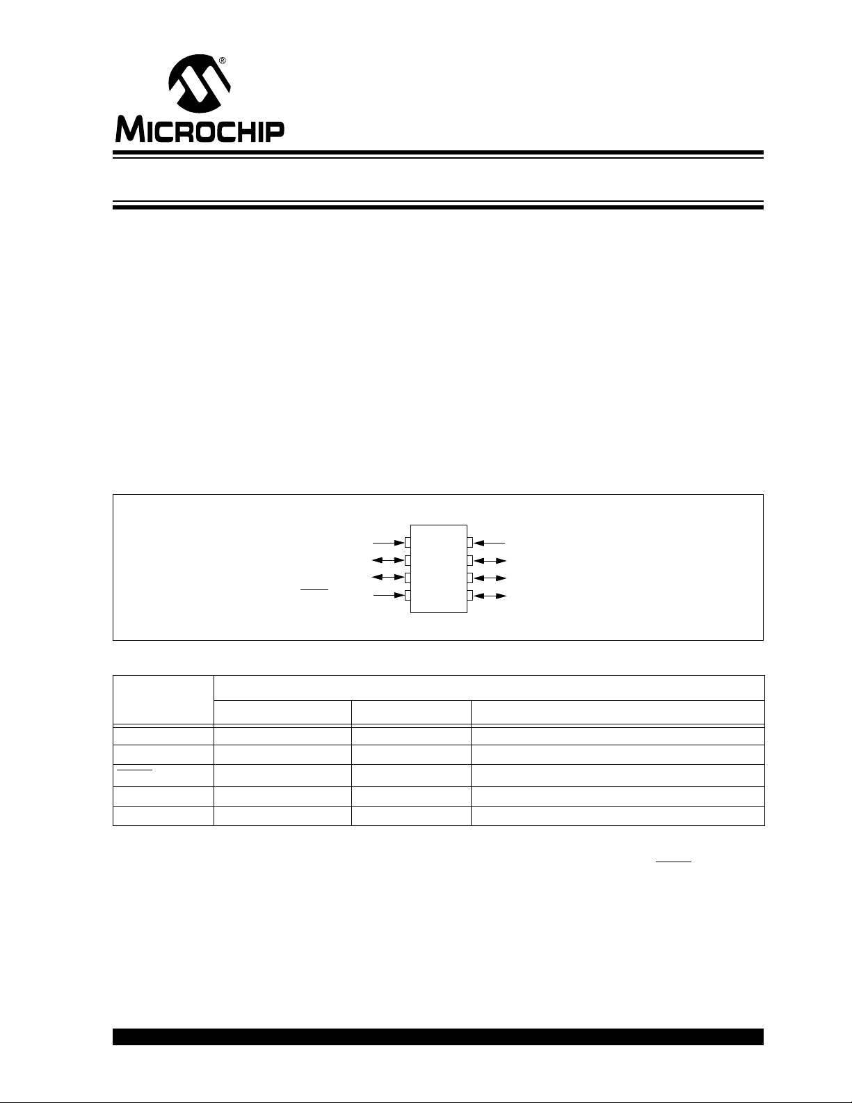
Pin Diagrams
TABLE 1-1: PIN DESCRIPTIONS (DURING PROGRAMMING): PIC12F510
Pin Name
During Programming
Function Pin Type Pin Description
GP1 ICSPCLK I Clock input – Schmitt Trigger input
GP0 ICSPDAT I/O Data input/output – Schmitt Trigger input
MCLR
/VPP/GP3 Program/Verify mode P
(1)
Program Mode Select
VDD VDD P Power Supply
V
SS VSS P Ground
Legend: I = Input, O = Output, P = Power
Note 1: In the PIC12F510, the programming high voltage is internally generated. To activate the Program/Verify
mode, high voltage of I
IHH current capability (see Table 6-1) needs to be applied to the MCLR input.
PDIP, SOIC, MSOP
VDD
GP5/OSC1/CLKIN
GP4/OSC2
MCLR
/VPP/GP3
1
2
3
4
VSS
GP0/AN0/CIN+/ICSPDAT
8
7
6
5
PIC12F510
GP1/AN1/CIN-/ICSPCLK
GP2/AN2/COUT//T0CKI
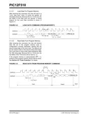
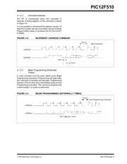
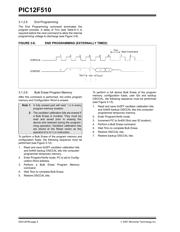
Memory Programming Specification
器件 Datasheet 文档搜索
AiEMA 数据库涵盖高达 72,405,303 个元件的数据手册,每天更新 5,000 多个 PDF 文件
