Datasheet 搜索 > 微控制器 > Microchip(微芯) > PIC12F615T-I/MF 数据手册 > PIC12F615T-I/MF 用户编程技术手册 6/28 页
 器件3D模型
¥ 8.941
PIC12F615T-I/MF 用户编程技术手册 - Microchip(微芯)
制造商:
Microchip(微芯)
分类:
微控制器
封装:
DFN-8
描述:
pic12 MCU 1.75kB 闪存 64 B RAM 6 I/O 内部振荡器 采用8引脚DFN封装
Pictures:
3D模型
符号图
焊盘图
引脚图
产品图
页面导航:
引脚图在P2Hot
电气规格在P24
导航目录
PIC12F615T-I/MF数据手册
Page:
of 28 Go
若手册格式错乱,请下载阅览PDF原文件
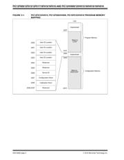
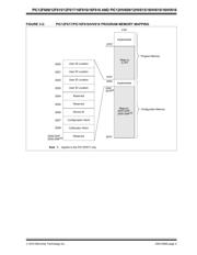
PIC12F609/12F615/12F617/16F610/16F616 AND PIC12HV609/12HV615/16HV610/16HV616
DS41284E-page 6 2010 Microchip Technology Inc.
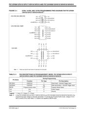
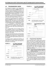
4.0 PROGRAM/VERIFY MODE
Two methods are available to enter Program/Verify
mode. “V
PP-first” is entered by holding ICSPDAT and
ICSPCLK low while raising the MCLR
pin from VIL to
V
IHH (high voltage), then applying VDD and data. This
method can be used for any Configuration Word selec-
tion and must be used if the INTOSC and internal
MCLR
options are selected (FOSC<2:0> = 100 or 101
and MCLRE = 0). The V
PP-first entry prevents the
device from executing code prior to entering Program/
Verify mode. See the timing diagram in Figure 4-1.
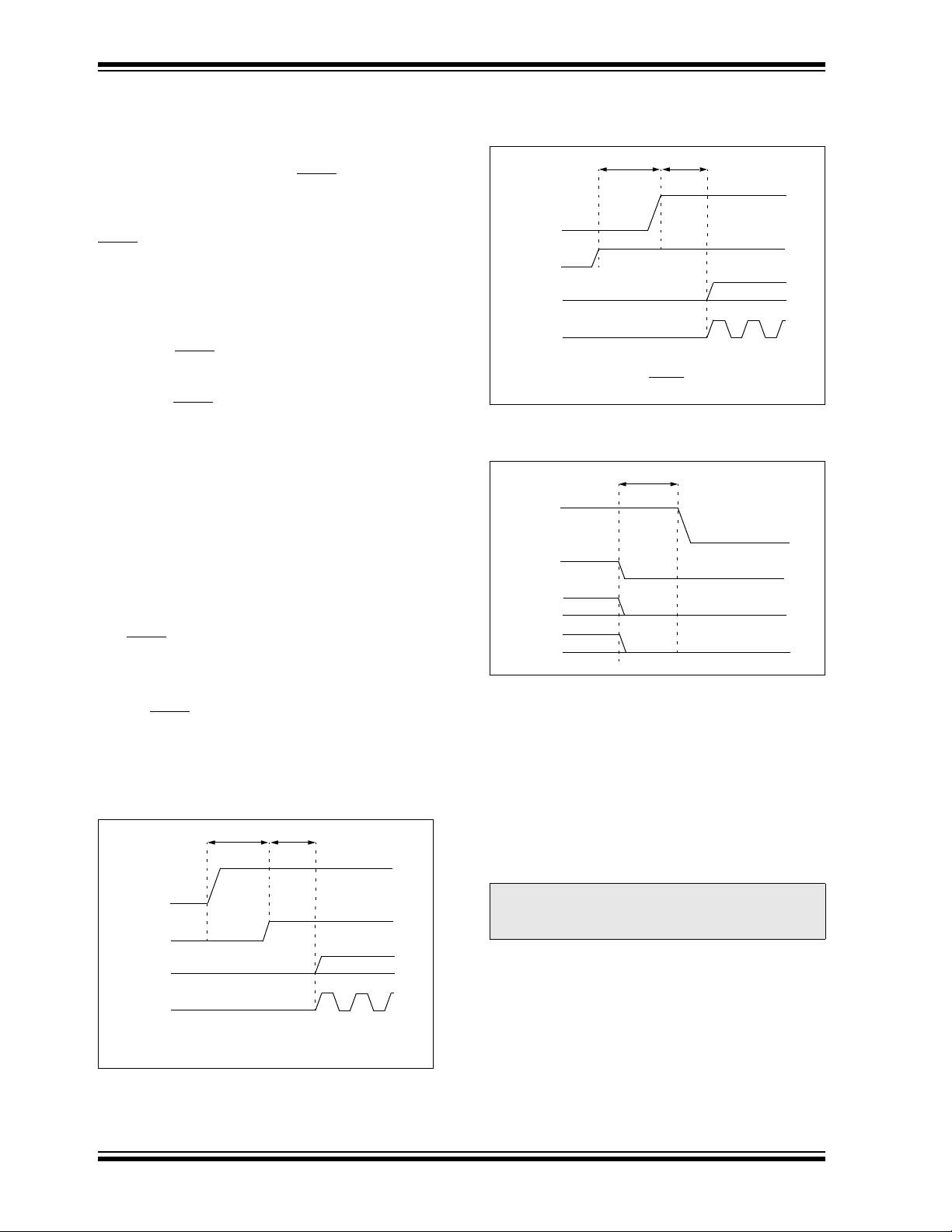
The second entry method, “V
DD-first”, is entered by
applying V
DD, holding ICSPDAT and ICSPCLK low,
then raising MCLR
pin from VIL to VIHH (high voltage),
followed by data. This method can be used for any
Configuration Word selection except when INTOSC
and internal MCLR
options are selected (FOSC<2:0> =
100 or 101 and MCLRE = 0). This technique is useful
when programming the device when VDD is already
applied, for it is not necessary to disconnect V
DD to
enter Program/Verify mode. See the timing diagram in
Figure 4-2.
Once in Program/Verify mode, the program memory
and configuration memory can be accessed and
programmed in serial fashion. ICSPDAT and ICSPCLK
are Schmitt Trigger inputs in this mode. RA4 is tri-state
regardless of fuse setting.
The sequence that enters the device into the Program/
Verify mode places all other logic into the Reset state
(the MCLR
pin was initially at VIL). Therefore, all I/Os
are in the Reset state (high-impedance inputs) and the
PC is cleared.
To prevent a device configured with INTOSC and
internal MCLR
from executing after exiting Program/
Verify mode, V
DD needs to power down before VPP.
See Figure 4-3 for the timing.
FIGURE 4-1: VPP-FIRST PROGRAM/
VERIFY MODE ENTRY
FIGURE 4-2: V
DD-FIRST PROGRAM/
VERIFY MODE ENTRY
FIGURE 4-3: PROGRAM/VERIFY MODE
EXIT
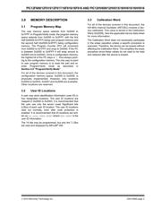
4.1 Program/Erase Algorithms
The PIC16F616/PIC12F617 program memory may be
written in two ways. The fastest method writes four
words at a time. However, one-word writes are also
supported for backward compatibility with previous 8-
pin and 14-pin Flash devices. The four-word algorithm
is used to program the program memory only. The one-
word algorithm can write any available memory
location (i.e., program memory, configuration memory
and calibration memory).
After writing the array, the PC may be reset and read
back to verify the write. It is not possible to verify
immediately following the write because the PC can
only increment, not decrement.
A device Reset will clear the PC and set the address to
‘0’. The Increment Address command will increment
the PC. The Load Configuration command will set the
PC to 0x2000. The available commands are shown in
Table 4-1.
VPP
THLD0
ICSPDAT
ICSPCLK
VDD
TPPDP
Note: This method of entry is valid, regardless
of Configuration Word selected.
Note: The PIC12F615, PIC12F609, PIC16F610
program memories must be written in
one-word writes only.
VPP
TPPDP
ICSPDAT
ICSPCLK
VDD
THLD0
Note: This method of entry is valid if INTOSC
and internal MCLR
are not selected.
VPP
ICSPDAT
ICSPCLK
VDD
THLD0
器件 Datasheet 文档搜索
AiEMA 数据库涵盖高达 72,405,303 个元件的数据手册,每天更新 5,000 多个 PDF 文件
