Datasheet 搜索 > 8位微控制器 > Microchip(微芯) > PIC16C55A-20I/P 数据手册 > PIC16C55A-20I/P 用户编程技术手册 4/29 页
 器件3D模型
¥ 21.413
PIC16C55A-20I/P 用户编程技术手册 - Microchip(微芯)
制造商:
Microchip(微芯)
分类:
8位微控制器
封装:
PDIP-28
描述:
MICROCHIP PIC16C55A-20I/P 微控制器, 8位, 一次性可编程, PIC16C5xx, 40 MHz, 768 Byte, 24 Byte, 28 引脚, DIP
Pictures:
3D模型
符号图
焊盘图
引脚图
产品图
页面导航:
导航目录
PIC16C55A-20I/P数据手册
Page:
of 29 Go
若手册格式错乱,请下载阅览PDF原文件
4
FN2969.5
April 4, 2005
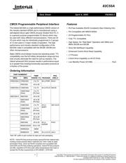
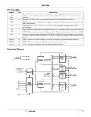
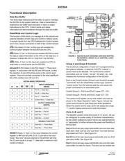
Functional Description
Data Bus Buffer
This three-state bidirectional 8-bit buffer is used to interface
the 82C55A to the system data bus. Data is transmitted or
received by the buffer upon execution of input or output
instructions by the CPU. Control words and status
information are also transferred through the data bus buffer.
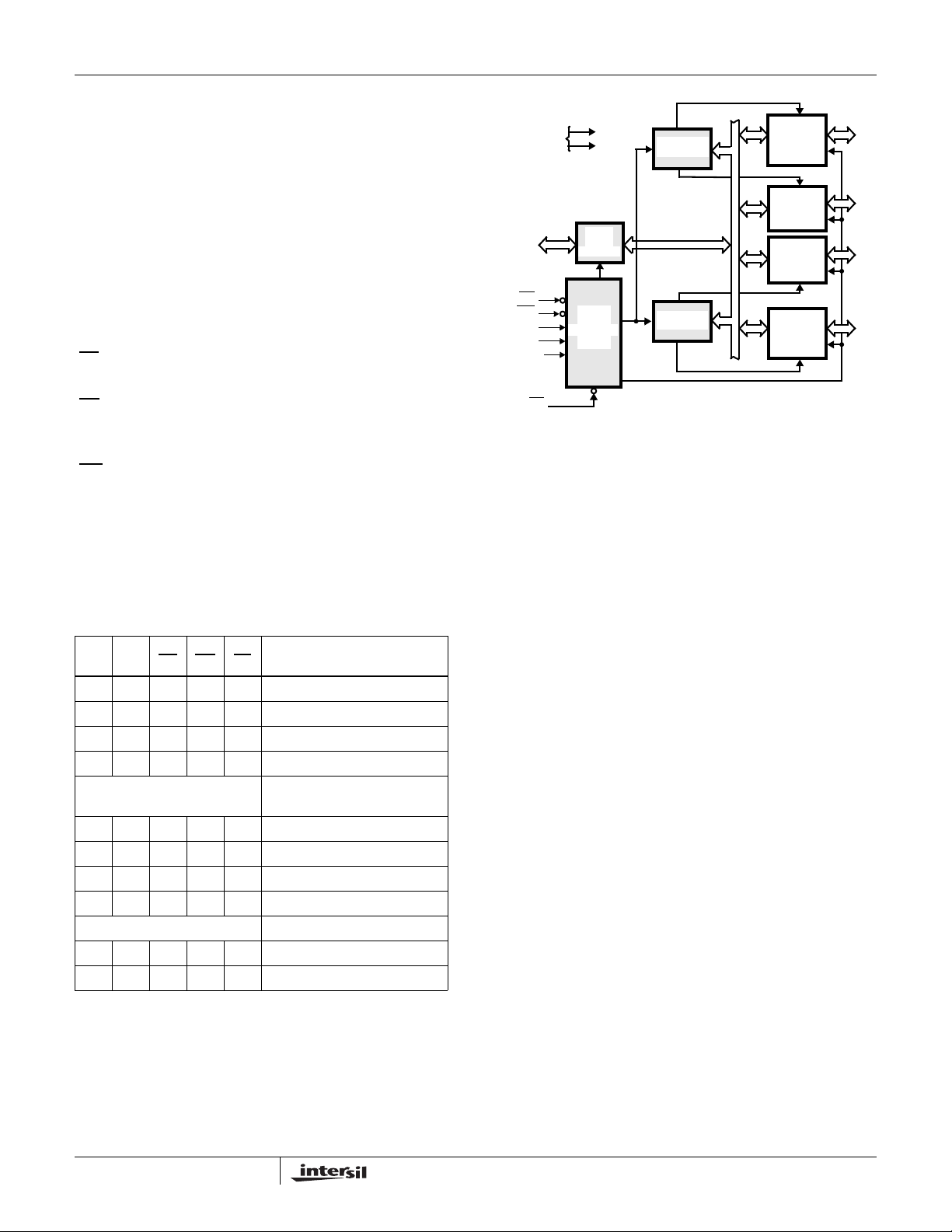
Read/Write and Control Logic
The function of this block is to manage all of the internal and
external transfers of both Data and Control or Status words.
It accepts inputs from the CPU Address and Control busses
and in turn, issues commands to both of the Control Groups.
(CS
) Chip Select. A “low” on this input pin enables the
communication between the 82C55A and the CPU.
(RD
) Read. A “low” on this input pin enables 82C55A to send
the data or status information to the CPU on the data bus. In
essence, it allows the CPU to “read from” the 82C55A.
(WR
) Write. A “low” on this input pin enables the CPU to
write data or control words into the 82C55A.
(A0 and A1) Port Select 0 and Port Select 1. These input
signals, in conjunction with the RD and WR inputs, control
the selection of one of the three ports or the control word
register. They are normally connected to the least significant
bits of the address bus (A0 and A1).
(RESET) Reset. A “high” on this input initializes the control
register to 9Bh and all ports (A, B, C) are set to the input
mode. “Bus hold” devices internal to the 82C55A will hold
the I/O port inputs to a logic “1” state with a maximum hold
current of 400µA.
Group A and Group B Controls
The functional configuration of each port is programmed by
the systems software. In essence, the CPU “outputs” a
control word to the 82C55A. The control word contains
information such as “mode”, “bit set”, “bit reset”, etc., that
initializes the functional configuration of the 82C55A.
Each of the Control blocks (Group A and Group B) accepts
“commands” from the Read/Write Control logic, receives
“control words” from the internal data bus and issues the
proper commands to its associated ports.
Control Group A - Port A and Port C upper (C7 - C4)
Control Group B - Port B and Port C lower (C3 - C0)
The control word register can be both written and read as
shown in the “Basic Operation” table. Figure 4 shows the
control word format for both Read and Write operations.
When the control word is read, bit D7 will always be a logic
“1”, as this implies control word mode information.
Ports A, B, and C
The 82C55A contains three 8-bit ports (A, B, and C). All can
be configured to a wide variety of functional characteristics
by the system software but each has its own special features
or “personality” to further enhance the power and flexibility of
the 82C55A.
Port A One 8-bit data output latch/buffer and one 8-bit data
input latch. Both “pull-up” and “pull-down” bus-hold devices
are present on Port A. See Figure 2A.
Port B One 8-bit data input/output latch/buffer and one 8-bit
data input buffer. See Figure 2B.
Port C One 8-bit data output latch/buffer and one 8-bit data
input buffer (no latch for input). This port can be divided into
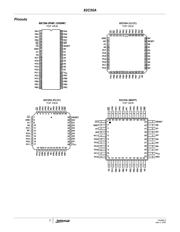
82C55A BASIC OPERATION
A1 A0 RD
WR CS
INPUT OPERATION
(READ)
00010Port A → Data Bus
01010Port B → Data Bus
10010Port C → Data Bus
11010Control Word → Data Bus
OUTPUT OPERATION
(WRITE)
00100Data Bus → Port A
01100Data Bus → Port B
10100Data Bus → Port C
11100Data Bus → Control
DISABLE FUNCTION
XXXX1Data Bus → Three-State
XX110Data Bus → Three-State
FIGURE 1. 82C55A BLOCK DIAGRAM. DATA BUS BUFFER,
READ/WRITE, GROUP A & B CONTROL LOGIC
FUNCTIONS
GROUP A
PORT A
(8)
GROUP A
PORT C
UPPER
(4)
GROUP B
PORT C
LOWER
(4)
GROUP B
PORT B
(8)
GROUP B
CONTROL
GROUP A
CONTROL
DATA
READ
WRITE
CONTROL
LOGIC
RD
WR
A1
A0
RESET
CS
D7-D0
POWER
SUPPLIES
+5V
GND
BIDIRECTIONAL
DATA BUS
I/O
PA7-
I/O
PC7-
I/O
PC3-
I/O
PB7-
BUFFER
BUS
PB0
PC0
PC4
PA0
8-BIT
INTERNAL
DATA BUS
82C55A
器件 Datasheet 文档搜索
AiEMA 数据库涵盖高达 72,405,303 个元件的数据手册,每天更新 5,000 多个 PDF 文件
