Datasheet 搜索 > 微控制器 > Microchip(微芯) > PIC16C55-RC/SO 数据手册 > PIC16C55-RC/SO 用户编程技术手册 2/16 页
 器件3D模型
¥ 18.739
PIC16C55-RC/SO 用户编程技术手册 - Microchip(微芯)
制造商:
Microchip(微芯)
分类:
微控制器
封装:
SOIC-28
描述:
PIC16 系列 24 B RAM 512 x 12位 EPROM 8位 CMOS 微控制器 - SOIC-28
Pictures:
3D模型
符号图
焊盘图
引脚图
产品图
页面导航:
引脚图在P1Hot
电气规格在P13


导航目录
PIC16C55-RC/SO数据手册
Page:
of 16 Go
若手册格式错乱,请下载阅览PDF原文件

PIC16C5XX
DS30190H-page 2 1999 Microchip Technology Inc.
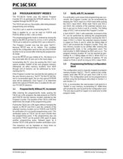
1.0 PROGRAM/VERIFY MODES
The PIC16C5X Series uses the internal Program
Counter (PC) to generate the EPROM address. V
PP is
supplied through the MCLR
pin.
The T0CKI pin acts as chip enable, alternating between
programming and verifying.
The OSC1 pin is used for incrementing the PC.
Data is applied to, or can be read on PORTA and
PORTB (MSB on RB7, LSB on RA0).
The programming/verify mode is entered by raising the
level on the MCLR
pin from VIL to VHH (= VPP) while the
T0CKI pin is held at V
IH and the OSC1 pin is held at VIL.
The Program Counter now has the value “0xFFF”,
because MCLR
was at VIL before. This condition
selects the configuration word as the very first EPROM
location to be accessed after entering the program/ver-
ify mode.
Since the MCLR
pin was initially at VIL, the device is in
the reset state (the I/O pins are in the reset state).
Incrementing the PC once (by pulsing the OSC1 pin)
selects location “0x000” of the user program memory.
Afterwards all other memory locations from 001h
through end of memory can be addressed by incre-
menting the PC.
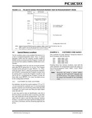
If the Program Counter has reached the last address of
the user memory area (e.g. “0x1FF” for the PIC16C54),
and is incremented again, the on-chip special EPROM
area will be addressed. (See Figure 1-2 to determine
where the special EPROM area is located for the vari-
ous PIC16C5X devices).
1.1 Program/Verify Without PC Increment
After entering the program/verify mode, pulsing the
T0CKI pin LOW programs the data present on PORTA
and PORTB into the memory location selected by the
Program Counter. The duration of the T0CKI LOW time
determines the length of the programming pulse.
Pulsing the T0CKI pin LOW again without changing the
signals on MCLR
and OSC1 puts the contents of the
selected memory location out on PORTA and PORTB
for verification of a successful programming cycle. This
verification pulse on T0CKI can be much shorter than
the programming pulse. If the programming was not
successful, T0CKI can be pulsed LOW again to apply
another programming pulse, followed again by a
shorter T0CKI LOW pulse for another verification cycle.
This sequence can be repeated as many times as
required until the programming is successful.
1.2 Verify with PC Increment
If a verification cycle shows that programming was suc-
cessful, the Program Counter can be incremented by
keeping the T0CKI input at a HIGH level while pulsing
the OSC1 input HIGH. When both T0CKI and OSC1
are HIGH, the contents of the selected memory loca-
tion is put out on Ports A and B (= Verify). The falling
edge of OSC1 will increment the Program Counter.
A fast VERIFY- ONLY with automatic increment of the
PC can be performed by entering the program/verify
mode as described above and then clocking the OSC1
input. If OSC1 is HIGH, the selected memory location
is output on Ports A and B, while the falling edge of
OSC1 will increment the Program Counter. Thus, the
first memory location to be verified after entering the
program/verify mode, is the configuration word. The
next location is 000h followed by 001h and so on. The
program memory location “N” can be reached by gen-
erating “N + 1” falling edges on OSC1. When OSC1 is
brought HIGH again, the contents of address “N” are
output on Ports A and B as long as OSC1 stays HIGH.
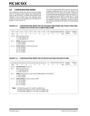
1.3 Programming/Verifying Configuration
Word
The configuration word is logically mapped at program
memory location “0xFFF”. The PC points to the config-
uration word after MCLR pin goes from LOW to VHH
(HIGH). The configuration word can be programmed or
verified using the techniques described in Section 1.1
and Section 1.2.
If PC is incremented, the next location it will point to is
“0x000” in user memory. Incrementing PC 4096 times
will not allow the user to point to the configuration word.
The only way to point to it again is to reset and re-enter
program mode.
器件 Datasheet 文档搜索
AiEMA 数据库涵盖高达 72,405,303 个元件的数据手册,每天更新 5,000 多个 PDF 文件
