Datasheet 搜索 > 微控制器 > Microchip(微芯) > PIC16C773/SP 数据手册 > PIC16C773/SP 用户编程技术手册 6/26 页
 器件3D模型
¥ 51.426
PIC16C773/SP 用户编程技术手册 - Microchip(微芯)
制造商:
Microchip(微芯)
分类:
微控制器
封装:
DIP-28
描述:
PIC16C773/774 8 位微控制器Microchip 的 PIC16C 系列微控制器 8 位 CMOS MCU,将 Microchip 的 PIC® 体系架构融入到引脚和封装选件中,从节省空间的 14 引脚设备到功能丰富的 64 引脚设备。 现在由基于闪存的型号代替,这些设备在传统设计方面也仍受到欢迎。 对于新应用,应考虑 PIC16F 型号。 PIC16C773/774 系列微控制器基于 Microchip 的中级体系结构,带 8 层硬件堆栈和 35 个 14 位指令。 这些 MCU 可提供高达 5 MIP、7 千字节的程序存储器,数据存储器为 256 字节 RAM。 板载 RC 振荡器,精确度为 ±1%。### 特点35 指令 8 级硬件堆栈 RC 振荡器 22 个输入/输出引脚 –PIC16C773 33 个输入/输出引脚 –PIC16C774 2 个捕获、比较、PWM (CCP) 模块 6 通道 12 位模拟到数字转换器 (ADC) - PIC16C773 10 通道 12 位模拟到数字转换器 (ADC) - PIC16C774 两个 8 位计时器 一个 16 位计时器 同步串行端口 (SSP),带有 SPI 和 I2C 通用同步异步接收器发送器 (USART/SCI) 并联从属端口 监控器计时器 (WDT) 通电重置 (POR) 通电计时器 (PWRT) 振荡器启动计时器 (OST) 掉电重置 (BOR) 在线串行编程 (ICSP) ### PIC16 微控制器展开
Pictures:
3D模型
符号图
焊盘图
引脚图
产品图
页面导航:
引脚图在P1P2P3Hot
技术参数、封装参数在P1

导航目录
PIC16C773/SP数据手册
Page:
of 26 Go
若手册格式错乱,请下载阅览PDF原文件
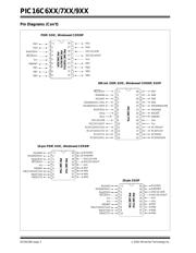
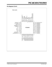
PIC16C6XX/7XX/9XX
DS30228K-page 6 2001 Microchip Technology Inc.
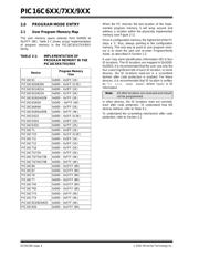
2.2 Program/Verify Mode
The Program/Verify mode is entered by holding pins
RB6 and RB7 low, while raising MCLR
pin from VSS to
the appropriate V
IHH (high voltage). Once in this mode,
the user program memory and the configuration mem-
ory can be accessed and programmed in serial fashion.
The mode of operation is serial, and the memory that is
accessed is the user program memory. RB6 is a
Schmitt Trigger input in this mode.
The sequence that enters the device into the
Programming/Verify mode places all other logic into the
RESET state (the MCLR
pin was initially at VSS). This
means that all I/O are in the RESET state (high
impedance inputs).
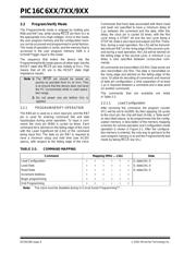
2.2.1 PROGRAM/VERIFY OPERATION
The RB6 pin is used as a clock input pin, and the RB7
pin is used for entering command bits and data
input/output during serial operation. To input a com-
mand, the clock pin (RB6) is cycled six times. Each
command bit is latched on the falling edge of the clock
with the Least Significant bit (LSb) of the command
being input first. The data on pin RB7 is required to
have a minimum setup and hold time (see AC/DC
specs), with respect to the falling edge of the clock.
Commands that have data associated with them (read
and load) are specified to have a minimum delay of
1 µs between the command and the data. After this
delay, the clock pin is cycled 16 times, with the first
cycle being a START bit and the last cycle being a
STOP bit. Data is also input and output LSb first. There-
fore, during a read operation, the LSb will be transmit-
ted onto pin RB7 on the rising edge of the second cycle,
and during a load operation, the LSb will be latched on
the falling edge of the second cycle. A minimum 1 µs
delay is also specified between consecutive com-
mands.
All commands are transmitted LSb first. Data words are
also transmitted LSb first. The data is transmitted on
the rising edge and latched on the falling edge of the
clock. To allow for decoding of commands and reversal
of data pin configuration, a time separation of at least
1 µs is required between a command and a data word
(or another command).
The commands that are available are listed
in Table 2-2.
2.2.1.1 Load Configuration
After receiving this command, the program counter
(PC) will be set to 0x2000. By then applying 16 cycles
to the clock pin, the chip will load 14-bits, a “data word”
as described above, to be programmed into the config-
uration memory. A description of the memory mapping
schemes for normal operation and Configuration mode
operation is shown in Figure 2-1. After the configura-
tion memory is entered, the only way to get back to the
user program memory is to exit the Program/Verify test
mode by taking MCLR
low (VIL).
TABLE 2-2: COMMAND MAPPING
Note 1: The MCLR pin should be raised as
quickly as possible from V
IL to VIHH. This
is to ensure that the device does not have
the PC incremented while in valid opera-
tion range.
2: Do not power any pin before V
DD is
applied.
Command Mapping (MSb ... LSb) Data
Load Configuration
000000
0, data(14), 0
Load Data
000010
0, data(14), 0
Read Data
000100
0, data(14), 0
Increment Address
000110
Begin programming
001000
End Programming
001110
Note: The clock must be disabled during In-Circuit Serial Programming
TM
.
器件 Datasheet 文档搜索
AiEMA 数据库涵盖高达 72,405,303 个元件的数据手册,每天更新 5,000 多个 PDF 文件
