Datasheet 搜索 > 8位微控制器 > Microchip(微芯) > PIC16F1708-I/SO 数据手册 > PIC16F1708-I/SO 用户编程技术手册 1/34 页
 器件3D模型
¥ 11.653
PIC16F1708-I/SO 用户编程技术手册 - Microchip(微芯)
制造商:
Microchip(微芯)
分类:
8位微控制器
封装:
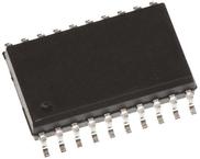
SOIC-20
描述:
MICROCHIP PIC16F1708-I/SO 微控制器, 8位, 闪存, PIC16F17xx, 32 MHz, 7 KB, 512 Byte, 20 引脚, SOIC
Pictures:
3D模型
符号图
焊盘图
引脚图
产品图
页面导航:
引脚图在P1Hot
技术参数、封装参数在P27
电气规格在P27

导航目录
PIC16F1708-I/SO数据手册
Page:
of 34 Go
若手册格式错乱,请下载阅览PDF原文件
2013 Microchip Technology Inc. DS41683A-page 1
PIC16(L)F1704/8
This document includes the
programming specifications for the
following devices:
1.0 OVERVIEW
The device can be programmed using either the high-
voltage In-Circuit Serial Programming™ (ICSP™)
method or the low-voltage ICSP method.
1.1 Hardware Requirements
1.1.1 HIGH-VOLTAGE ICSP
PROGRAMMING
In High-Voltage ICSP mode, the device requires two
programmable power supplies: one for V
DD and one for
the MCLR
/VPP pin.
1.1.2 LOW-VOLTAGE ICSP
PROGRAMMING
In Low-Voltage ICSP mode, the PIC16(L)F1704/8
devices can be programmed using a single V
DD source
in the operating range. The MCLR
/VPP pin does not
have to be brought to a different voltage, but can
instead be left at the normal operating voltage.
1.1.2.1 Single-Supply ICSP Programming
The LVP bit in Configuration Word 2 enables single-
supply (low-voltage) ICSP programming. The LVP bit
defaults to a ‘1’ (enabled) from the factory. The LVP bit
may only be programmed to ‘0’ by entering the High-
Voltage ICSP mode, where the MCLR
/VPP pin is raised
to V
IHH. Once the LVP bit is programmed to a ‘0’, only
the High-Voltage ICSP mode is available and only the
High-Voltage ICSP mode can be used to program the
device.
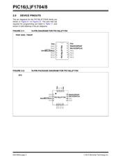
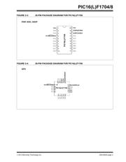
1.2 Pin Utilization
Five pins are needed for ICSP programming. The pins
are listed in Ta ble 1 -1.
• PIC16F1704 • PIC16LF1704
• PIC16F1708 • PIC16LF1708
Note 1: The High-Voltage ICSP mode is always
available, regardless of the state of the
LVP bit, by applying V
IHH to the MCLR/
V
PP pin.
2: While in Low-Voltage ICSP mode, MCLR
is always enabled, regardless of the
MCLRE bit, and the port pin can no
longer be used as a general purpose
input.
TABLE 1-1: PIN DESCRIPTIONS DURING PROGRAMMING FOR PIC16(L)F1704/8
Pin Name
During Programming
Function Pin Type Pin Description
RA1 ICSPCLK I Clock Input – Schmitt Trigger Input
RA0 ICSPDAT I/O Data Input/Output – Schmitt Trigger Input
RA3/MCLR
/VPP Program/Verify mode P
(1)
Program Mode Select/Programming Power Supply
VDD VDD P Power Supply
V
SS VSS P Ground
Legend: I = Input, O = Output, P = Power
Note 1: The programming high voltage is internally generated. To activate the Program/Verify mode, high voltage
needs to be applied to MCLR input. Since the MCLR is used for a level source, MCLR does not draw any
significant current.
PIC16(L)F1704/8 Memory Programming Specification
器件 Datasheet 文档搜索
AiEMA 数据库涵盖高达 72,405,303 个元件的数据手册,每天更新 5,000 多个 PDF 文件
