Datasheet 搜索 > 8位微控制器 > Microchip(微芯) > PIC16F1769-E/P 数据手册 > PIC16F1769-E/P 用户编程技术手册 3/16 页
 器件3D模型
¥ 0.834
PIC16F1769-E/P 用户编程技术手册 - Microchip(微芯)
制造商:
Microchip(微芯)
分类:
8位微控制器
封装:
PDIP-20
描述:
8位微控制器 -MCU 8-Bit MCU 14KB Flash 1KB RAM 10bit DAC
Pictures:
3D模型
符号图
焊盘图
引脚图
产品图
页面导航:
原理图在P1
应用领域在P10
导航目录
PIC16F1769-E/P数据手册
Page:
of 16 Go
若手册格式错乱,请下载阅览PDF原文件

2016 Microchip Technology Inc. DS90003140B-page 3
TB3140
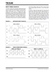
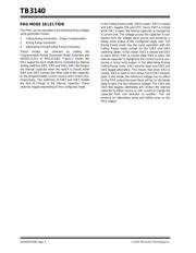
Aside from the selectable timing input sources and the
polarity event, the input timing source detection method
can also be selected. The two event input detection
methods for PRG are level sensitive and edge
sensitive. The set rising and set falling input detection
are selected by setting the Set Rising Input Mode
Select bit (REDG) and Set Falling Input Mode Select bit
(FEDG) in the PRGxCON0 register, respectively. In
general, edge-sensitive operation is useful when timing
inputs are derived from periodic sources while level-
sensitive operation is useful when timing inputs are
derived from voltage thresholds.
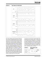
The timing sources for the PRG may vary from device
to device. Some of the available peripherals that can be
used as PRG’s timing sources are Comparator, PWM
(Pulse-Width Modulation) and CCP (Capture,
Compare, PWM) output. The peripheral must be
configured beforehand and selected as the PRG’s
timing source. For a device that has Peripheral Pin
Select (PPS), the PRGxR and PRGxF are remapped to
the desired input pins through the PPS Input Selection
Register (xxxPPS). By changing the “xxx” notation in
the register name to PRGxR and PRGxF, any available
I/O pin can be selected as PRGxR and PRGxF. For
example, in order to use RA0 and RA1 as the PRGxR
pin and PRGxF pin respectively, the xxxPPS becomes
PRGxRPPS and PRGxFPPS. This register should be
set to a corresponding value defined in the data sheet
to assign RA0 and RA1 as PRGxR pin and PRGxF pin.
Voltage Input Source
The PRG’s voltage input source serves as a voltage
reference to the linear ramp output. The input source
can be any of the following: external source from the
PRGxIN0 or PRGxIN1 pins, the buffered output of the
internal Fixed Voltage Reference (FVR), or one of the
internal Digital-to-Analog Converters (DAC). The op
amp outputs share the PRGxIN0 and PRGxIN1 pins so
that the reference signal can be buffered by the op amp
by enabling both the op amp and selecting the
corresponding PRGxIN pin. Reference sources are
selected by setting the Voltage Input Select bits
(INS<2:0>) in the PRGxINS register.
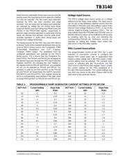
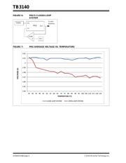
PRG Current Source/Sink
The programmable current on the PRG has a vast
selection of source/sink currents to configure the
desired PRG output slope rate. In applications that
require a steep voltage rate in the PRG output, a high-
current setting must be selected. The constant ramp
current is selected with the Source/Sink Set bits
(ISET<3:0>) in the PRGxCON2 register. Table 1 shows
the current settings for the PRG peripheral of a
PIC16F1769 microcontroller. The current settings may
vary from one device to the other. Please refer to the
data sheet of the particular device.
TABLE 1: PROGRAMMABLE RAMP GENERATOR CURRENT SETTINGS OF PIC16F1769
ISET<4:0> Current Setting
(µA)
Slope Rate
(V/µs)
ISET<4:0> Current Setting
(µA)
Slope Rate
(V/µs)
0h 2 0.2 10h 10 1.0
1h 2.5 0.25 11h 11 1.1
2h 3 0.3 12h 12 1.2
3h 3.5 0.35 13h 13 1.3
4h 4 0.4 14h 14 1.4
5h 4.5 0.45 15h 15 1.5
6h 5 0.5 16h 16 1.6
7h 5.5 0.55 17h 17 1.7
8h 6 0.6 18h 18 1.8
9h 6.5 0.65 19h 19 1.9
Ah 7 0.7 1Ah 20 2
Bh 7.5 0.75 1Bh 21 2.1
Ch 8 0.8 1Ch 22 2.2
Dh 8.5 0.85 1Dh 23 2.3
Eh 9 0.9 1Eh 24 2.4
Fh 9.5 0.95 1Fh 25 2.5
器件 Datasheet 文档搜索
AiEMA 数据库涵盖高达 72,405,303 个元件的数据手册,每天更新 5,000 多个 PDF 文件
