Datasheet 搜索 > 8位微控制器 > Microchip(微芯) > PIC16F616-E/ST 数据手册 > PIC16F616-E/ST 用户编程技术手册 3/28 页
 器件3D模型
¥ 11.972
PIC16F616-E/ST 用户编程技术手册 - Microchip(微芯)
制造商:
Microchip(微芯)
分类:
8位微控制器
封装:
TSSOP-14
描述:
PIC16F610/616 8 位闪存微控制器Microchip 的 PIC16F 系列微控制器 8 位 MCU,将 Microchip 的 PIC® 体系架构融入到引脚和封装选件中,从节省空间的 14 引脚设备到功能丰富的 64 引脚设备。 带有基线、中级或增强型中级体系架构的设备提供多种不同的外围设备组合,可谓设计人员提供灵活性,并为应用提供选择。 PIC16F610/616 系列微控制器基于 Microchip 的中级内核,带 8 层深硬件堆栈和 35 个指令。 这些 MCU 提供高达 5 个 MIP、3.5 千字节程序存储器、128 字节 RAM 和 128 字节数据 EEPROM。 板载是一个可配置振荡器,工厂校准到 ±1% 精确度。### 微控制器功能最大 20 MHz CPU 速度 35 指令 8 级硬件堆栈 8 MHz 内部振荡器 - 可选频率范围 4 MHz 或 8 MHz 11 个输入/输出引脚 通电重置 (POR) 通电计时器 (PWRT) 振荡器启动计时器 (OST) 掉电重置 (BOR) 监控器计时器 (WDT) 在线串行编程 (ICSP) ### 外设8 通道 10 位模拟到数字转换器 – 仅限 PIC16F616 型号 两个比较器 8 位计时器 - PIC16F610 x 1、PIC16F616 x 2 一个 16 位计时器 ### PIC16 微控制器展开
Pictures:
3D模型
符号图
焊盘图
引脚图
产品图
页面导航:
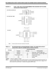
引脚图在P2Hot
电气规格在P24
导航目录
PIC16F616-E/ST数据手册
Page:
of 28 Go
若手册格式错乱,请下载阅览PDF原文件

2010 Microchip Technology Inc. DS41284E-page 3
PIC12F609/12F615/12F617/16F610/16F616 AND PIC12HV609/12HV615/16HV610/16HV616
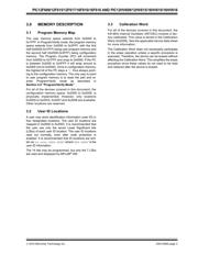
3.0 MEMORY DESCRIPTION
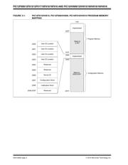
3.1 Program Memory Map
The user memory space extends from 0x0000 to
0x1FFF. In Program/Verify mode, the program memory
space extends from 0x0000 to 0x3FFF, with the first
half (0x0000-0x1FFF) being user program memory and
the second half (0x2000-0x3FFF) being configuration
memory. The Program Counter (PC) will increment
from 0x0000 to 0x1FFF and wrap to 0x0000. If the PC
is between 0x2000 to 0x3FFF it will wrap around to
0x2000 (not to 0x0000). Once in configuration memory,
the highest bit of the PC stays a ‘1’, thus always point-
ing to the configuration memory. The only way to point
to user program memory is to reset the part and re-
enter Program/Verify mode as described in
Section 4.0 “Program/Verify Mode”.
For all of the devices covered in this document, the
configuration memory space, 0x2000 to 0x2008, is
physically implemented. However, only locations
0x2000 to 0x2003, 0x2007 and 0x2008 are available.
Other locations are reserved.
3.2 User ID Locations
A user may store identification information (user ID) in
four designated locations. The user ID locations are
mapped in 0x2000 to 0x2003. It is recommended that
the user use only the seven Least Significant bits
(LSbs) of each user ID location. The user ID locations
read out normally, even after code protection is
enabled. It is recommended that ID locations are writ-
ten as ‘xx xxxx xbbb bbbb’ where ‘bbb bbbb’ is the
user ID information.
The 14 bits may be programmed, but only the 7 LSbs
are read and displayed by MPLAB
®
IDE.
3.3 Calibration Word
For all of the devices covered in this document, the
4/8 MHz Internal Oscillator (INTOSC) module is fac-
tory calibrated. This value is stored in the Calibration
Word (0x2008). See the applicable device data sheet
for more information.
The Calibration Word does not necessarily participate
in the erase operation unless a specific procedure is
executed. Therefore, the device can be erased without
affecting the Calibration Word. This simplifies the erase
procedure since these values do not need to be read
and restored after the device is erased.
器件 Datasheet 文档搜索
AiEMA 数据库涵盖高达 72,405,303 个元件的数据手册,每天更新 5,000 多个 PDF 文件
