Datasheet 搜索 > 微控制器 > Microchip(微芯) > PIC16F676-I/SL 数据手册 > PIC16F676-I/SL 用户编程技术手册 6/24 页
 器件3D模型
¥ 4.401
PIC16F676-I/SL 用户编程技术手册 - Microchip(微芯)
制造商:
Microchip(微芯)
分类:
微控制器
封装:
SOIC-14
描述:
MICROCHIP PIC16F676-I/SL 微控制器, 8位, 闪存, AEC-Q100, PIC16F, 20 MHz, 1.75 KB, 64 Byte, 14 引脚, SOIC
Pictures:
3D模型
符号图
焊盘图
引脚图
产品图
页面导航:
引脚图在P1P2P3Hot
电气规格在P21

导航目录
PIC16F676-I/SL数据手册
Page:
of 24 Go
若手册格式错乱,请下载阅览PDF原文件
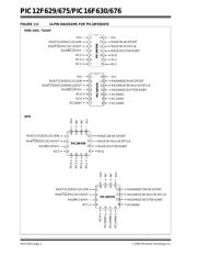
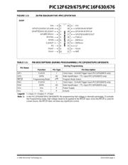
PIC12F629/675/PIC16F630/676
DS41191D-page 6 © 2005 Microchip Technology Inc.
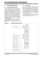
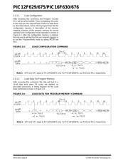
2.3.1.1 Load Configuration
After receiving this command, the Program Counter
(PC) will be set to 0x2000. Then, by applying 16 cycles
to the clock pin, the chip will load 14 bits in a data word,
as described above, which will be programmed into the
configuration memory. A description of the memory
mapping schemes of the program memory for normal
operation and Configuration mode operation is shown in
Figure 2-3. After the configuration memory is entered,
the only way to get back to the user program memory is
to exit the Program/Verify mode by taking MCLR
low
(V
IL).
FIGURE 2-3: LOAD CONFIGURATION COMMAND
2.3.1.2 Load Data For Program Memory
After receiving this command, the chip will load in a
14-bit data word when 16 cycles are applied, as
described previously. A timing diagram for the Load
Data command is shown in Figure 2-4.
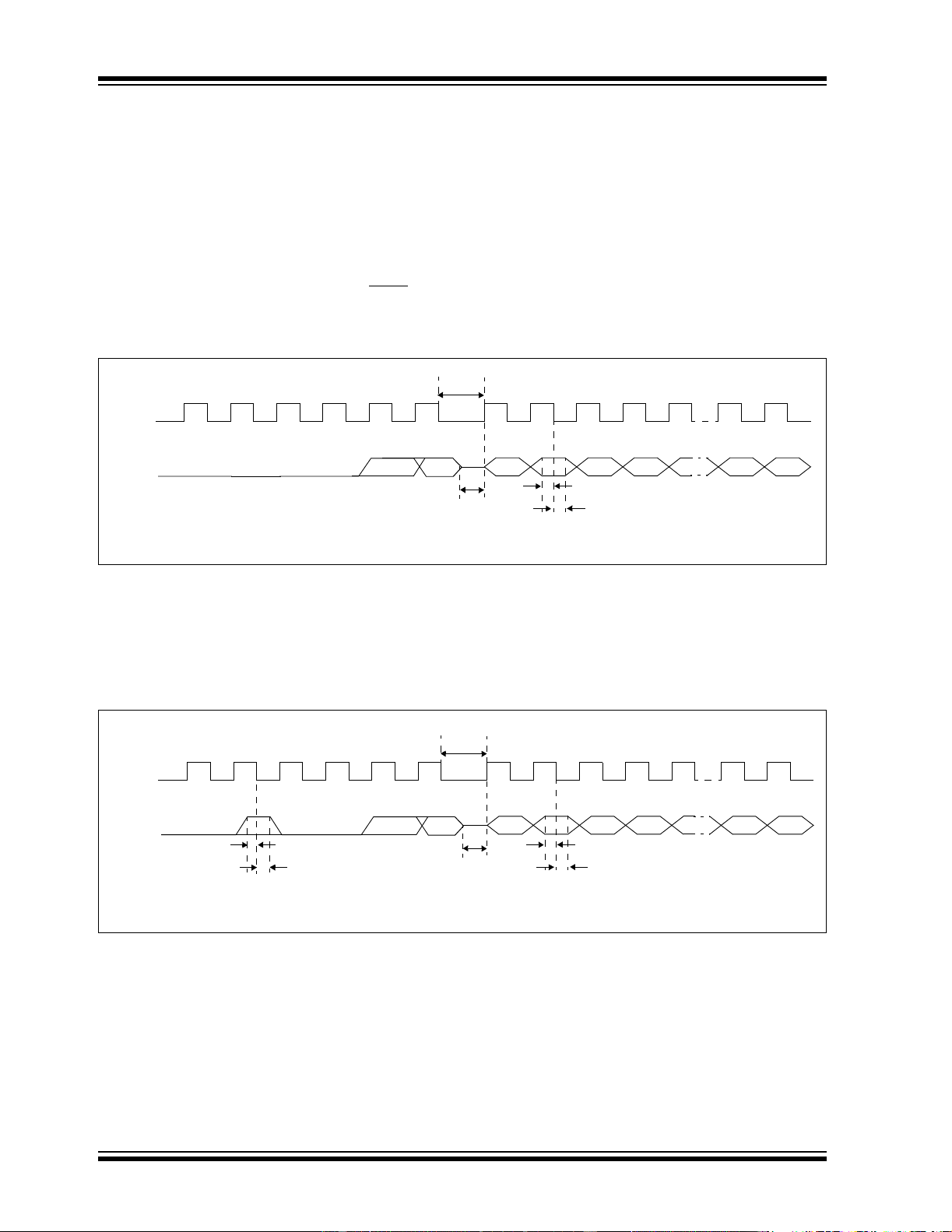
FIGURE 2-4: LOAD DATA FOR PROGRAM MEMORY COMMAND
TSET1
T
HLD1
T
DLY1
T
DLY2
12 34 56
0 0 0
0
x
x
12 34 5 15
16
strt_bit
stp_bit
LSb MSb
0
GP1
(1)
GP0
(1)
CLOCK
DATA
Note 1: GP0 and GP1 apply to PIC12F629/675 only. For PIC16F630/676, use RA0 and RA1, respectively.
TSET1
T
HLD1
T
DLY1
TDLY2
12 34 56
0 0
0
x
x
12 34 5 15
16
strt_bit
stp_bit
LSb MSb
GP1
(1)
CLOCK
TSET1
T
HLD1
0
1
GP0
(1)
DATA
Note 1: GP0 and GP1 apply to PIC12F629/675 only. For PIC16F630/676, use RA0 and RA1, respectively.
器件 Datasheet 文档搜索
AiEMA 数据库涵盖高达 72,405,303 个元件的数据手册,每天更新 5,000 多个 PDF 文件
