Datasheet 搜索 > 8位微控制器 > Microchip(微芯) > PIC16F73T-I/SO 数据手册 > PIC16F73T-I/SO 用户编程技术手册 5/16 页
 器件3D模型
¥ 38.43
PIC16F73T-I/SO 用户编程技术手册 - Microchip(微芯)
制造商:
Microchip(微芯)
分类:
8位微控制器
封装:
SOIC-28
描述:
MICROCHIP PIC16F73T-I/SO 微控制器, 8位, 闪存, PIC16F, 20 MHz, 7 KB, 192 Byte, 28 引脚, SOIC
Pictures:
3D模型
符号图
焊盘图
引脚图
产品图
页面导航:
引脚图在P1Hot
电气规格在P12
导航目录
PIC16F73T-I/SO数据手册
Page:
of 16 Go
若手册格式错乱,请下载阅览PDF原文件

2002 Microchip Technology Inc. DS30324B-page 5
PIC16F7X
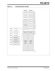
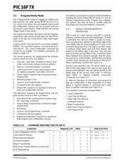
2.3.1.1 Load Configuration
After receiving the Load Configuration command, the
PC will be set to 0x2000 and the data sent with the
command is discarded. The four ID locations and the
configuration word can then be programmed using the
normal programming sequence, as described in
Section 2.3. A description of the memory mapping
schemes of the program memory for normal operation
and Configuration mode operation is shown in
Figure 2-1. After the configuration memory is entered,
the only way to get back to the user program memory
is to exit the Program/Verify Test mode by taking MCLR
low.
2.3.1.2 Load Data for Memory
The device will load in a 14-bit “data word” (LSb first)
when 16 cycles are applied, as described previously. A
timing diagram for the load data command is shown in
Figure 5-1.
2.3.1.3 Read Data from Memory
The device will transmit data bits out of the memory
(program or configuration) currently addressed by the
PC, starting with the second rising edge of the clock
input. RB7 will go into Output mode on the second ris-
ing clock edge and will revert back to Input mode (hi-
impedance) after the 16th rising edge. Data is sent out
LSb first. A timing diagram for this command is shown
in Figure 5-2.
If the device is code protected, user program memory
will read all ‘0’s. Configuration memory can still be read.
2.3.1.4 Increment Address
The PC is incremented by one. A timing diagram for
this command is shown in Figure 5-3.
2.3.1.5 Begin Programming
A ‘Load Data’ command must be issued before
every ‘Begin Programming’ command. Program-
ming of memory (configuration or program) will begin
after this command is received and decoded. Program-
ming requires (tprog) time and is terminated using an
‘End Programming’ command.
2.3.1.6 Chip Erase (Program Memory)
Erasure of configuration and program memory begins
after this command is received and decoded. The
erase sequence is self-timed and it is not necessary to
issue an ‘End Programming’ command, only to wait for
the appropriate time interval (tera) for the entire erase
sequence, before issuing another command.
This procedure will disable code protection (code pro-
tect bit = 1); however, all data within the program mem-
ory will be erased when this command is executed and
thus, the security of the data or code is not
compromised.
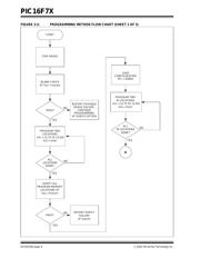
2.4 Programming Algorithm Requires
Variable V
DD
The PIC16F7X uses an intelligent algorithm. The algo-
rithm calls for program verification at V
DDAPP.
The actual chip erase and programming must be done
with V
DD in the VDDP range (See Table 5-1).
V
DDP =VDD range required during programming
V
DDAPP =VDD in the target application
Programmers must verify the PIC16F7X at V
DDAPP.
Since Microchip may introduce future versions of the
PIC16F7X with a broader VDD range, it is best that
these levels are user selectable (defaults are OK).
Note: All CHIP ERASE operations must take
place with V
DD between 4.75V and 5.25V
(i.e., V
DDP).
Note: Any programmer not meeting this require-
ment may only be classified as a “proto-
type” or “development” programmer, but
not a “production quality” programmer.
器件 Datasheet 文档搜索
AiEMA 数据库涵盖高达 72,405,303 个元件的数据手册,每天更新 5,000 多个 PDF 文件
