Datasheet 搜索 > 微控制器 > Microchip(微芯) > PIC16F84A-04I/SO 数据手册 > PIC16F84A-04I/SO 用户编程技术手册 3/16 页
 器件3D模型
¥ 6.232
PIC16F84A-04I/SO 用户编程技术手册 - Microchip(微芯)
制造商:
Microchip(微芯)
分类:
微控制器
封装:
SOIC-18
描述:
MICROCHIP PIC16F84A-04I/SO 微控制器, 8位, 闪存, PIC16F, 4 MHz, 1.75 KB, 68 Byte, 18 引脚, SOIC
Pictures:
3D模型
符号图
焊盘图
引脚图
产品图
页面导航:
引脚图在P1Hot
电气规格在P3
导航目录
PIC16F84A-04I/SO数据手册
Page:
of 16 Go
若手册格式错乱,请下载阅览PDF原文件

2002 Microchip Technology Inc. DS30262E-page 3
PIC16F8X
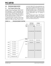
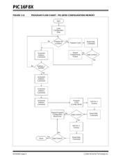
2.2 ID Locations
A user may store identification information (ID) in four
ID locations, mapped in addresses 2000h through
2003h. It is recommended that the user use only the
four Least Significant bits of each ID location. The ID
locations read out in an unscrambled fashion after code
protection is enabled. It is recommended that ID loca-
tion is written as “11 1111 1000 bbbb”, where
“bbbb” is ID information.
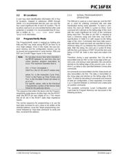
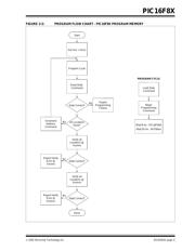
2.3 Program/Verify Mode
The Program/Verify mode is entered by holding pins
RB6 and RB7 low, while raising MCLR
pin from VIL to
V
IHH (high voltage). Once in this mode, the user pro-
gram memory and the configuration memory can be
accessed and programmed in serial fashion. RB6 and
RB7 are Schmitt Trigger inputs in this mode.
The sequence that enters the device into the Program-
ming/Verify mode places all other logic into the RESET
state (the MCLR
pin was initially at VIL). This means
that all I/O are in the RESET state (high impedance
inputs).
The normal sequence for programming is to use the
load data command to set a value to be written at the
selected address. Issue the “begin programming com-
mand” followed by “read data command” to verify and
then, increment the address.
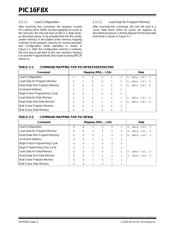
2.3.1 SERIAL PROGRAM/VERIFY
OPERATION
The RB6 pin is used as a clock input pin, and the RB7
pin is used for entering command bits and data
input/output during serial operation. To input a com-
mand, the clock pin (RB6) is cycled six times. Each
command bit is latched on the falling edge of the clock
with the Least Significant bit (LSb) of the command
being input first. The data on pin RB7 is required to
have a minimum setup and hold time (see AC/DC
specifications in Table 5-1), with respect to the falling
edge of the clock. Commands that have data associ-
ated with them (read and load) are specified to have a
minimum delay of 1 µs between the command and the
data. After this delay, the clock pin is cycled 16 times
with the first cycle being a START bit and the last cycle
being a STOP bit. Data is also input and output LSb
first.
Therefore, during a read operation, the LSb will be
transmitted onto pin RB7 on the rising edge of the sec-
ond cycle, and during a load operation, the LSb will be
latched on the falling edge of the second cycle. A min-
imum 1 µs delay is also specified between consecutive
commands.
All commands are transmitted LSb first. Data words are
also transmitted LSb first. The data is transmitted on
the rising edge and latched on the falling edge of the
clock. To allow for decoding of commands and reversal
of data pin configuration, a time separation of at least
1 µs is required between a command and a data word
(or another command).
The available commands (Load Configuration and
Load Data for Program Memory) are discussed in the
following sections.
Note: Do not allow excess time when transition-
ing MCLR
between VIL and VIHH; this can
cause spurious program executions to
occur. The maximum transition time is
1TCY + TPWRT (if enabled) +
1024 T
OSC (for LP, HS and XT modes only)
where TCY is the Instruction Cycle Time,
T
PWRT is the Power-up Timer Period, and
T
OSC is the Oscillator Period (all values in
µs or ns).
For specific values, refer to the Electrical
Characteristics section of the Device Data
Sheet for the particular device.
器件 Datasheet 文档搜索
AiEMA 数据库涵盖高达 72,405,303 个元件的数据手册,每天更新 5,000 多个 PDF 文件
