Datasheet 搜索 > 微控制器 > Microchip(微芯) > PIC16F877A-E/ML 数据手册 > PIC16F877A-E/ML 用户编程技术手册 5/22 页
 器件3D模型
¥ 70.866
PIC16F877A-E/ML 用户编程技术手册 - Microchip(微芯)
制造商:
Microchip(微芯)
分类:
微控制器
封装:
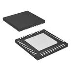
QFN-44
描述:
8位微控制器 -MCU 14KB 368 RAM 33 I/O
Pictures:
3D模型
符号图
焊盘图
引脚图
产品图
页面导航:
引脚图在P1P2Hot
电气规格在P16
导航目录
PIC16F877A-E/ML数据手册
Page:
of 22 Go
若手册格式错乱,请下载阅览PDF原文件

2010 Microchip Technology Inc. Advance Information DS39589C-page 5
PIC16F87XA
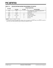
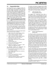
2.4 Program/Verify Mode
The Program/Verify mode is entered by holding pins
RB6 and RB7 low, while raising MCLR
pin from VIL to
V
IHH (high voltage). In this mode, the state of the RB3
pin does not effect programming. Low Voltage ICSP
Programming mode is entered by raising RB3 from VIL
to VDD, and then applying VDD to MCLR. Once in this
mode, the user program memory and the configuration
memory can be accessed and programmed in serial
fashion. The mode of operation is serial, and the mem-
ory accessed is the user program memory. RB6 and
RB7 are Schmitt Trigger inputs in this mode.
The sequence that enters the device into the Program-
ming/Verify mode places all other logic into the RESET
state (the MCLR
pin was initially at VIL). This means all
I/O are in the RESET state (high impedance inputs).
A device RESET will clear the PC and set the address
to ‘0’. The ‘Increment Address’ command will incre-
ment the PC. The ‘Load Configuration’ command will
set the PC to 2000h. The available commands are
shown in Table 2-1.
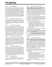
The normal sequence for programming eight program
memory words at a time is as follows:
1. Load a word at the current program memory
address using the ‘Load Data’ command.
2. Issue an ‘Increment Address’ command.
3. Load a word at the current program memory
address using the ‘Load Data’ command.
4. Repeat Step 2 and Step 3 six times.
5. Issue a ‘Begin Programming’ command to begin
programming.
6. Wait tprog (about 1 ms).
7. Issue an ‘End Programming’ command.
8. Increment to the next address.
9. Repeat this sequence as required to write
program and configuration memory.
The alternative sequence for programming one
program memory word at a time is as follows:
1. Set a word for the current memory location using
the ‘Load Data’ command.
2. Issue a ‘Begin Programming Only’ command to
begin programming.
3. Wait tprog.
4. Issue an ‘End Programming’ command.
5. Increment to the next address.
6. Repeat this alternative sequence as required to
write program and configuration memory.
The address and program counter are reset to 0000h
by resetting the device (taking MCLR
below VIL) and
re-entering Programming mode. Program and configu-
ration memory may then be read or verified using the
‘Read Data’ and ‘Increment Address’ commands.
2.4.1 LOW VOLTAGE ICSP
PROGRAMMING MODE
Low Voltage ICSP Programming mode allows a
PIC16F87XA device to be programmed using V
DD
only. However, when this mode is enabled by a config-
uration bit (LVP), the PIC16F87XA device dedicates
RB3 to control entry/exit into Programming mode.
When LVP bit is set to ‘1’, the low voltage ICSP pro-
gramming entry is enabled. Since the LVP configura-
tion bit allows low voltage ICSP programming entry in
its erased state, an erased device will have the LVP bit
enabled at the factory. While LVP is ‘1’, RB3 is dedi-
cated to low voltage ICSP programming. Bring RB3
and then, MCLR
to VDD to enter Programming mode.
All other specifications for high voltage ICSP apply.
To disable Low Voltage ICSP mode, the LVP bit must
be programmed to ‘0’. This must be done while entered
with the High Voltage Entry mode (LVP bit = ‘1’). RB3
is now a general purpose I/O pin.
2.4.2 SERIAL PROGRAM/VERIFY
OPERATION
The RB6 pin is used as a clock input pin, and the RB7
pin is used to enter command bits, and to input or out-
put data during serial operation. To input a command,
the clock pin (RB6) is cycled six times. Each command
bit is latched on the falling edge of the clock, with the
Least Significant bit (LSb) of the command being input
first. The data on RB7 is required to have a minimum
setup (tset1) and hold (thold1) time (see AC/DC speci-
fications), with respect to the falling edge of the clock.
Commands with associated data (read and load) are
specified to have a minimum delay (tdly1) of 1 s
between the command and the data. After this delay,
the clock pin is cycled 16 times, with the first cycle
being a Start bit (0) and the last cycle being a Stop bit
(0). Data is transferred LSb first.
During a read operation, the LSb will be transmitted
onto RB7 on the rising edge of the second cycle, and
during a load operation, the LSb will be latched on the
falling edge of the second cycle. A minimum 1 s delay
(tdly2) is specified between consecutive commands.
All commands and data words are transmitted LSb first.
The data is transmitted on the rising edge, and latched
on the falling edge of the clock. To allow decoding of
commands and reversal of data pin configuration, a
time separation of at least 1 s (tdly1) is required
between a command and a data word, or another
command.
The available commands are described in the following
paragraphs and listed in Table 2-1.
Note: The OSC must not have 72 osc clocks
while the device MCLR
is between VIL and
V
IHH.
器件 Datasheet 文档搜索
AiEMA 数据库涵盖高达 72,405,303 个元件的数据手册,每天更新 5,000 多个 PDF 文件
