Datasheet 搜索 > 微控制器 > Microchip(微芯) > PIC16LF1824T39AT-I/ST 数据手册 > PIC16LF1824T39AT-I/ST 用户编程技术手册 1/6 页
 器件3D模型
¥ 18.551
PIC16LF1824T39AT-I/ST 用户编程技术手册 - Microchip(微芯)
制造商:
Microchip(微芯)
分类:
微控制器
封装:
TSSOP-20
描述:
PIC16F 系列 256 B RAM 7 kB 闪存 8-位 表面贴装 微控制器-TSSOP-20
Pictures:
3D模型
符号图
焊盘图
引脚图
产品图
页面导航:
引脚图在P1Hot
功能描述在P1
导航目录
PIC16LF1824T39AT-I/ST数据手册
Page:
of 6 Go
若手册格式错乱,请下载阅览PDF原文件
2012 Microchip Technology Inc. Advance Information DS41654A-page 1
PIC16LF1824T39A
This document includes the
programming specifications for the
following device:
1.0 OVERVIEW
The PIC16LF1824T39A is a dual-die device containing
a Microchip PIC16LF1824 microcontroller and an
integrated transmitter. The dies are electrically
isolated.
Since the microcontroller portion of this device is a stan-
dard PIC16LF1824, programming should be done
according to its programming specification,
“PIC12(L)F1822/PIC16(L)F182X Memory Programming
Specification” (DS41390).
The transmitter contains no user-programmable
memory.
Care should be taken to prevent the transmitter from
transmitting during the programming cycle. In-Circuit
Serial Programming™ (ICSP™) pins should not be
connected to the DATA pin. If the transmitter V
DD
supply is separate from the microcontroller, it should be
kept at V
SS during the programming cycle.
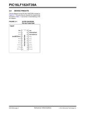
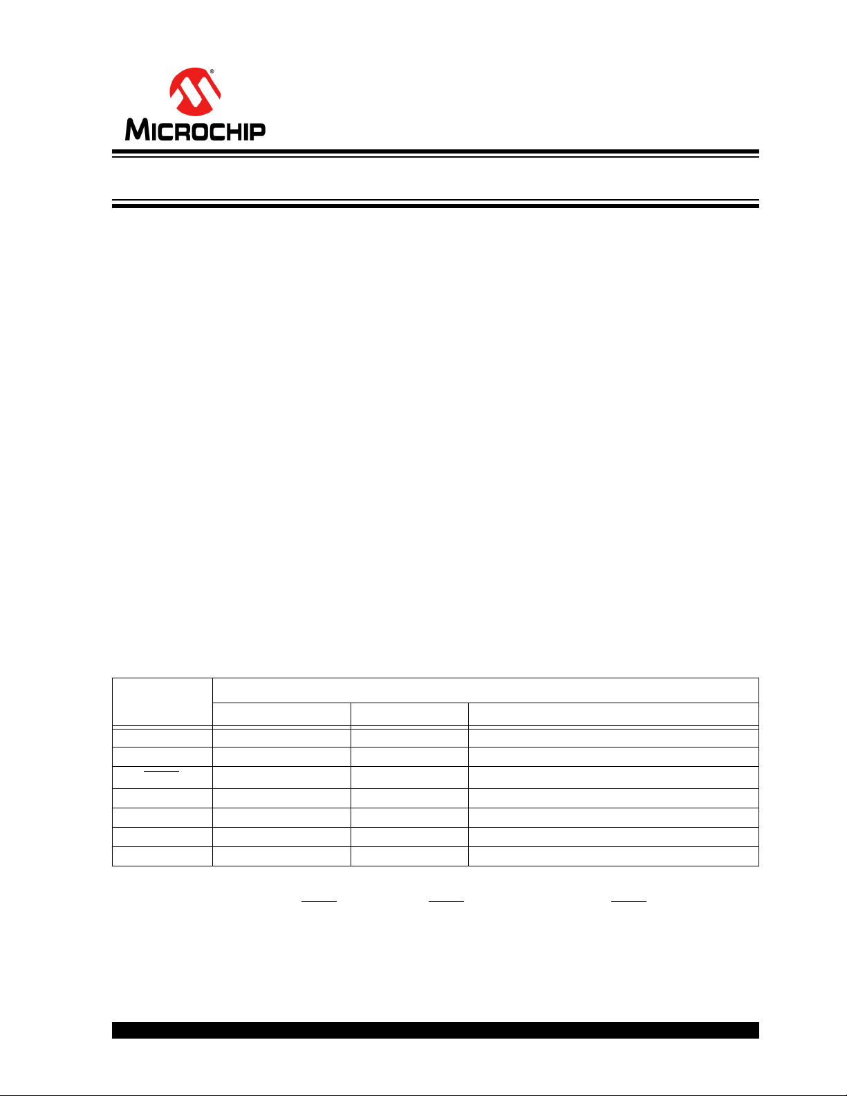
1.1 Pin Utilization
Five pins are needed for ICSP™ programming. Two
additional pins should be connected to ground during
programming. The pins are listed in Table 1-1.
TABLE 1-1: PIN DESCRIPTIONS DURING PROGRAMMING
• PIC16LF1824T39A
Pin Name
During Programming
Function Pin Type Pin Description
RA1 ICSPCLK I/O Clock Input – Schmitt Trigger Input
RA0 ICSPDAT I/O Data Input/Output – Schmitt Trigger Input
RA3/MCLR
/VPP Program/Verify mode P
(1)
Program mode Select/Programming Power Supply
V
DD VDD P Microcontroller Power Supply
VSS VSS P Microcontroller Ground
VDDRF VDD P RF Power Supply
V
SSRF VSS P RF Ground
Legend: I = Input, O = Output, P = Power
Note 1: The programming high voltage is internally generated. To activate the Program/Verify mode, high voltage
needs to be applied to MCLR
input. Since the MCLR is used for a level source, MCLR does not draw any
significant current.
PIC16LF1824T39A Programming Specification
器件 Datasheet 文档搜索
AiEMA 数据库涵盖高达 72,405,303 个元件的数据手册,每天更新 5,000 多个 PDF 文件
