Datasheet 搜索 > 微控制器 > Microchip(微芯) > PIC16LF876A-I/SP 数据手册 > PIC16LF876A-I/SP 用户编程技术手册 6/22 页
 器件3D模型
¥ 45.914
PIC16LF876A-I/SP 用户编程技术手册 - Microchip(微芯)
制造商:
Microchip(微芯)
分类:
微控制器
封装:
DIP-28
描述:
MICROCHIP PIC16LF876A-I/SP. 微控制器, 8位, PIC16LF8xx, 20 MHz, 14 KB, 368 Byte, 28 引脚, NDIP
Pictures:
3D模型
符号图
焊盘图
引脚图
产品图
页面导航:
引脚图在P1P2Hot
电气规格在P16
导航目录
PIC16LF876A-I/SP数据手册
Page:
of 22 Go
若手册格式错乱,请下载阅览PDF原文件

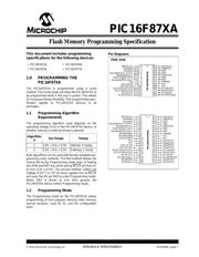
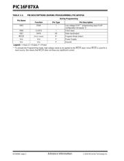
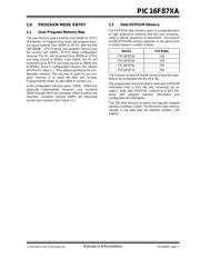
PIC16F87XA
DS39589C-page 6 Advance Information 2010 Microchip Technology Inc.
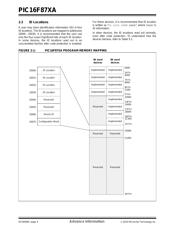
2.4.2.1 Load Configuration
After receiving this command, the program counter
(PC) will be set to 2000h. By then applying 16 cycles to
the clock pin, the chip will load 14 bits in a “data word,”
as described above, to be programmed into the config-
uration memory. A description of the memory mapping
schemes of the program memory for normal operation
and configuration mode operation is shown in
Figure 2-1. After the configuration memory is entered,
the only way to get back to the user program memory
is to exit the Program/Verify Test mode by taking MCLR
low (VIL).
2.4.2.2 Load Data for Program Memory
After receiving this command, the chip will load one
word (with 14 bits as a “data word”) to be programmed
into user program memory when 16 cycles are applied.
A timing diagram for this command is shown in
Figure 6-1.
2.4.2.3 Load Data for Data Memory
After receiving this command, the chip will load in a
14-bit “data word” when 16 cycles are applied.
However, the data memory is only 8-bits wide, and
thus, only the first 8 bits of data after the Start bit will be
programmed into the data memory. It is still necessary
to cycle the clock the full 16 cycles in order to allow the
internal circuitry to reset properly. The data memory
contains up to 256 bytes. If the device is
code-protected, the data is read as all zeros. A timing
diagram for this command is shown in Figure 6-2.
2.4.2.4 Read Data from Program Memory
After receiving this command, the chip will transmit
data bits out of the program memory (user or configu-
ration) currently accessed, starting with the second ris-
ing edge of the clock input. The RB7 pin will go into
Output mode on the second rising clock edge, and it
will revert back to Input mode (high-impedance) after
the 16th rising edge. A timing diagram of this command
is shown in Figure 6-3.
2.4.2.5 Read Data from Data Memory
After receiving this command, the chip will transmit
data bits out of the data memory, starting with the sec-
ond rising edge of the clock input. The RB7 pin will go
into Output mode on the second rising edge, and it will
revert back to Input mode (high-impedance) after the
16th rising edge. As previously stated, the data mem-
ory is 8-bits wide, and therefore, only the first 8 bits that
are output are actual data. A timing diagram for this
command is shown in Figure 6-4.
2.4.2.6 Increment Address
The PC is incremented when this command is
received. A timing diagram of this command is shown
in Figure 6-5.
2.4.2.7 Begin Erase/Program Cycle
Eight locations must be loaded before every
‘Begin Erase/Programming’ command. After this
command is received and decoded, eight words of
program memory will be erased and programmed with
the values contained in the program data latches. The
PC address will decode which eight words are pro-
grammed. The lower three bits of the PC are ignored,
so if the PC points to address 003h, then all eight
locations from 000h to 007h are written.
An internal timing mechanism executes an erase
before write. The user must allow the combined time
for erase and programming, as specified in the electri-
cal specs, for programming to complete. No ‘End
Programming’ command is required.
1. If the address is pointing to user memory, the
user memory alone will be affected.
2. If the address is pointing to the physically imple-
mented test memory (2000h - 201Fh), test mem-
ory will be written. The configuration word will not
be written unless the address is specifically
pointing to 2007h.
This command can be used to perform programming
over the entire V
DD range of the device.
A timing diagram for this command is shown in
Figure 6-6.
2.4.2.8 Begin Programming Only
This command is similar to the ‘Erase/Programming
Cycle’ command, except that a word erase is not
done, and the internal timer is not used. Programming
of program and data memory will begin after this com-
mand is received and decoded. The user must allow
the time for programming, as specified in the electrical
specs, for programming to complete. An ‘End
Programming’ command is required.
The internal timer is not used for this command, so the
‘End Programming’ command must be used to stop
programming.
1. If the address is pointing to user memory, the
user memory alone will be affected.
2. If the address is pointing to the physically imple-
mented test memory (2000h - 201Fh), the test
memory will be written. The configuration word
will not be written unless the address is
specifically pointing to 2007h.
A timing diagram for this command is shown in
Figure 6-7.
Note 1: The code-protect bits cannot be erased
with this command.
2: All Begin Erase/Programming operations
can take place over the entire V
DD range.
Note: Begin Programming Only operations must
take place at the 4.5V to 5.5V V
DD range.
器件 Datasheet 文档搜索
AiEMA 数据库涵盖高达 72,405,303 个元件的数据手册,每天更新 5,000 多个 PDF 文件
