Datasheet 搜索 > 微控制器 > Microchip(微芯) > PIC18F2420-I/SP 数据手册 > PIC18F2420-I/SP 用户编程技术手册 1/46 页
 器件3D模型
¥ 33.801
PIC18F2420-I/SP 用户编程技术手册 - Microchip(微芯)
制造商:
Microchip(微芯)
分类:
微控制器
封装:
DIP-28
描述:
PIC18F2420/2520/4420/4520 8 位微控制器Microchip 的 PIC18F 微控制器是 Microchip 产品线中功能最强大的 8 位设备。 该系列包含的 CAN、LIN 和以太网功能是完整系列外围设备的一部分,可满足嵌入式应用和版本的需求,采用 XLP(极低功耗)技术,用于功耗为关键考量的应用。 PIC18F2420/2520/4420/4520 系列微控制器基于 Microchip 的 PIC18 体系结构,提供 31 级 硬件堆栈和 75 指令。 这些 MCU 提供高达 10 个 MIPS、多达 64 kb 的程序存储器、多达 3896 kb 的 RAM。 板载可配置振荡器。### 微控制器功能40 MHz 最大 CPU 速度 75 指令 - 通过扩展指令集支持 83 指令 31 级硬件堆栈 可配置内部振荡器 - 可选频率范围 8 mHz 至 31 kHz 25 个输入/输出引脚 - PIC18F2420/2520 型号 36 个输入/输出引脚 - PIC18F4420/4520 型号 nanoWatt 技术 通电重置 (POR) 通电计时器 (PWRT) 振荡器启动计时器 (OST) 掉电重置 (BOR) 延长监控计时器 (WDT) 高电压/低电压检测 (HLVD) 模块 低电压编程 (LVP) 在线串行编程 (ICSP) 在线调试 (ICD) ### 外设10 位模拟到数字转换器 (ADC) - PIC18F2420/2520 型号 10 通道;PIC18F4420/4520 13 通道 一个增强型采集、比较、PWM 模块 - 仅 PIC18F4420/4520 型号 采集、比较、PWM 模块 - PIC18F2420/2520 型号 x 2、PIC18F4420/4520 型号 x 1 两个比较器 一个 8 位计时器 三个 16 位计时器 主同步串行端口 (MSSP) 模块,带有 SPI 和 I2C 增强型可寻址通用同步异步接收器发送器 (EUSART) ### PIC18 微控制器展开
Pictures:
3D模型
符号图
焊盘图
引脚图
产品图
页面导航:
引脚图在P1P2P3P13Hot
电气规格在P42P43
导航目录
PIC18F2420-I/SP数据手册
Page:
of 46 Go
若手册格式错乱,请下载阅览PDF原文件
2010 Microchip Technology Inc. DS39622L-page 1
PIC18F2XXX/4XXX FAMILY
1.0 DEVICE OVERVIEW
This document includes the programming specifications
for the following devices:
2.0 PROGRAMMING OVERVIEW
PIC18F2XXX/4XXX family devices can be
programmed using either the high-voltage In-Circuit
Serial Programming™ (ICSP™) method or the
low-voltage ICSP method. Both methods can be done
with the device in the user’s system. The low-voltage
ICSP method is slightly different than the high-voltage
method and these differences are noted where
applicable.
This programming specification applies to the
PIC18F2XXX/4XXX family devices in all package
types.
2.1 Hardware Requirements
In High-Voltage ICSP mode, PIC18F2XXX/4XXX
family devices require two programmable power sup-
plies: one for VDD and one for MCLR/VPP/RE3. Both
supplies should have a minimum resolution of 0.25V.
Refer to Section 6.0 “AC/DC Characteristics Timing
Requirements for Program/Verify Test Mode” for
additional hardware parameters.
2.1.1 LOW-VOLTAGE ICSP
PROGRAMMING
In Low-Voltage ICSP mode, PIC18F2XXX/4XXX
family devices can be programmed using a V
DD
source in the operating range. The MCLR/VPP/RE3
does not have to be brought to a different voltage, but
can instead be left at the normal operating voltage.
Refer to Section 6.0 “AC/DC Characteristics Timing
Requirements for Program/Verify Test Mode” for
additional hardware parameters.
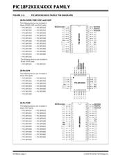
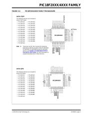
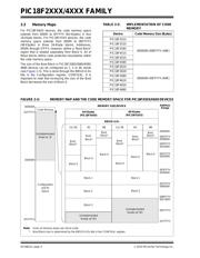
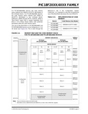
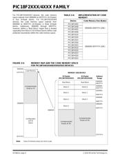
2.2 Pin Diagrams
The pin diagrams for the PIC18F2XXX/4XXX family
are shown in Figure 2-1 and Figure 2-2.
TABLE 2-1: PIN DESCRIPTIONS (DURING PROGRAMMING): PIC18F2XXX/4XXX FAMILY
• PIC18F2221 • PIC18F2580 • PIC18F4480
• PIC18F2321 • PIC18F2585 • PIC18F4510
• PIC18F2410 • PIC18F2610 • PIC18F4515
• PIC18F2420 • PIC18F2620 • PIC18F4520
• PIC18F2423 • PIC18F2680 • PIC18F4523
• PIC18F2450 • PIC18F2682 • PIC18F4525
• PIC18F2455 • PIC18F2685 • PIC18F4550
• PIC18F2458 • PIC18F4221 • PIC18F4553
• PIC18F2480 • PIC18F4321 • PIC18F4580
• PIC18F2510 • PIC18F4410 • PIC18F4585
• PIC18F2515 • PIC18F4420 • PIC18F4610
• PIC18F2520 • PIC18F4423 • PIC18F4620
• PIC18F2523 • PIC18F4450 • PIC18F4680
• PIC18F2525 • PIC18F4455 • PIC18F4682
• PIC18F2550 • PIC18F4458 • PIC18F4685
•PIC18F2553
Pin Name
During Programming
Pin Name Pin Type Pin Description
MCLR
/VPP/RE3 VPP P Programming Enable
V
DD
(2)
VDD P Power Supply
V
SS
(2)
VSS P Ground
RB5 PGM I Low-Voltage ICSP™ Input when LVP
Configuration bit equals ‘1’
(1)
RB6 PGC I Serial Clock
RB7 PGD I/O Serial Data
Legend: I = Input, O = Output, P = Power
Note 1: See Figure 5-1 for more information.
2: All power supply (V
DD) and ground (VSS) pins must be connected.
Flash Microcontroller Programming Specification
器件 Datasheet 文档搜索
AiEMA 数据库涵盖高达 72,405,303 个元件的数据手册,每天更新 5,000 多个 PDF 文件
