Datasheet 搜索 > 微控制器 > Microchip(微芯) > PIC18F2423T-I/SO 数据手册 > PIC18F2423T-I/SO 用户编程技术手册 1/34 页
 器件3D模型
¥ 49.653
PIC18F2423T-I/SO 用户编程技术手册 - Microchip(微芯)
制造商:
Microchip(微芯)
分类:
微控制器
封装:
SOIC-28
描述:
PIC 40MHz 闪存:8K@x16bit
Pictures:
3D模型
符号图
焊盘图
引脚图
产品图
页面导航:
引脚图在P1P2P3Hot
电气规格在P30P31
导航目录
PIC18F2423T-I/SO数据手册
Page:
of 34 Go
若手册格式错乱,请下载阅览PDF原文件
© 2005 Microchip Technology Inc. DS39759A-page 1
PIC18F2423/2523/4423/4523
1.0 DEVICE OVERVIEW
This document includes the programming specifications
for the following devices:
2.0 PROGRAMMING OVERVIEW
PIC18F2423/2523/4423/4523 devices can be
programmed using either the high-voltage In-Circuit
Serial Programming™ (ICSP™) method or the
low-voltage ICSP method. Both methods can be done
with the device in the users’ system. The low-voltage
ICSP method is slightly different than the high-voltage
method and these differences are noted where
applicable.
This programming specification applies to
PIC18F2423/2523/4423/4523 devices in all package
types.
2.1 Hardware Requirements
In High-Voltage ICSP mode, PIC18F2423/2523/4423/
4523 devices require two programmable power sup-
plies: one for VDD and one for MCLR/VPP/RE3. Both
supplies should have a minimum resolution of 0.25V.
Refer to Section 6.0 “AC/DC Characteristics Timing
Requirements for Program/Verify Test Mode” for
additional hardware parameters.
2.1.1 LOW-VOLTAGE ICSP
PROGRAMMING
In Low-Voltage ICSP mode, PIC18F2423/2523/4423/
4523 devices can be programmed using a V
DD source
in the operating range. The MCLR
/VPP/RE3 pin does
not have to be brought to a different voltage, but can
instead be left at the normal operating voltage. Refer to
Section 6.0 “AC/DC Characteristics Timing
Requirements for Program/Verify Test Mode” for
additional hardware parameters.
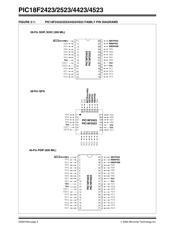
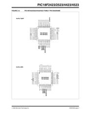
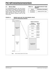
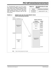
2.2 Pin Diagrams
The pin diagrams for the PIC18F2423/2523/4423/4523
family are shown in Figure 2-1 and Figure 2-2.
TABLE 2-1: PIN DESCRIPTIONS (DURING PROGRAMMING): PIC18F2423/2523/4423/4523
• PIC18F2423 • PIC18F4423
• PIC18F2523 • PIC18F4523
Pin Name
During Programming
Pin Name Pin Type Pin Description
MCLR
/VPP/RE3 VPP P Programming Enable
V
DD
(2)
VDD P Power Supply
V
SS
(2)
VSS P Ground
RB5 PGM I Low-Voltage ICSP™ Input when LVP
Configuration bit equals ‘1’
(1)
RB6 PGC I Serial Clock
RB7 PGD I/O Serial Data
Legend: I = Input, O = Output, P = Power
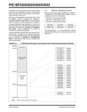
Note 1: See Figure 5-1
for more information.
2: All power supply (V
DD) and ground (VSS) pins must be connected.
Flash Microcontroller Programming Specification
器件 Datasheet 文档搜索
AiEMA 数据库涵盖高达 72,405,303 个元件的数据手册,每天更新 5,000 多个 PDF 文件
