Datasheet 搜索 > 微控制器 > Microchip(微芯) > PIC24F08KA101T-I/MQ 数据手册 > PIC24F08KA101T-I/MQ 用户编程技术手册 4/54 页

 器件3D模型
¥ 19.187
PIC24F08KA101T-I/MQ 用户编程技术手册 - Microchip(微芯)
制造商:
Microchip(微芯)
分类:
微控制器
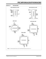
封装:
QFN-20
描述:
16位微控制器 - MCU 8KB Flash 1KB RAM 16-bit PIC24F Family
Pictures:
3D模型
符号图
焊盘图
引脚图
产品图
页面导航:
引脚图在P2P3Hot
技术参数、封装参数在P1
导航目录
PIC24F08KA101T-I/MQ数据手册
Page:
of 54 Go
若手册格式错乱,请下载阅览PDF原文件
PIC24FXXKA1XX/FVXXKA3XX
DS39919C-page 4 2008-2012 Microchip Technology Inc.
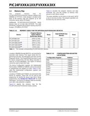
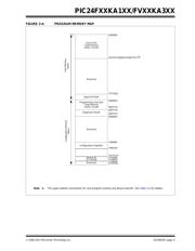
2.2 Memory Map
The program memory map for
PIC24FXXKA1XX/FVXXKA3XX devices extends from
000000h to FFFFFEh. Code storage is located at the
base of the memory map and supports up to 11K
instruction words (about 32 Kbytes).
Additionally, PIC24FXXKA1XX/FVXXKA3XX family
devices have an on-chip data EEPROM. This data
EEPROM is mapped to the program memory area from
location, 7FFE00h to 7FFFFEh.
Table 2-2 provides the program memory and data
EEPROM size, and the number of memory rows
present in each device variant.
The erase operation can be done on one word, half of
a row or one row at a time. The program operation can
be done only one word at a time.
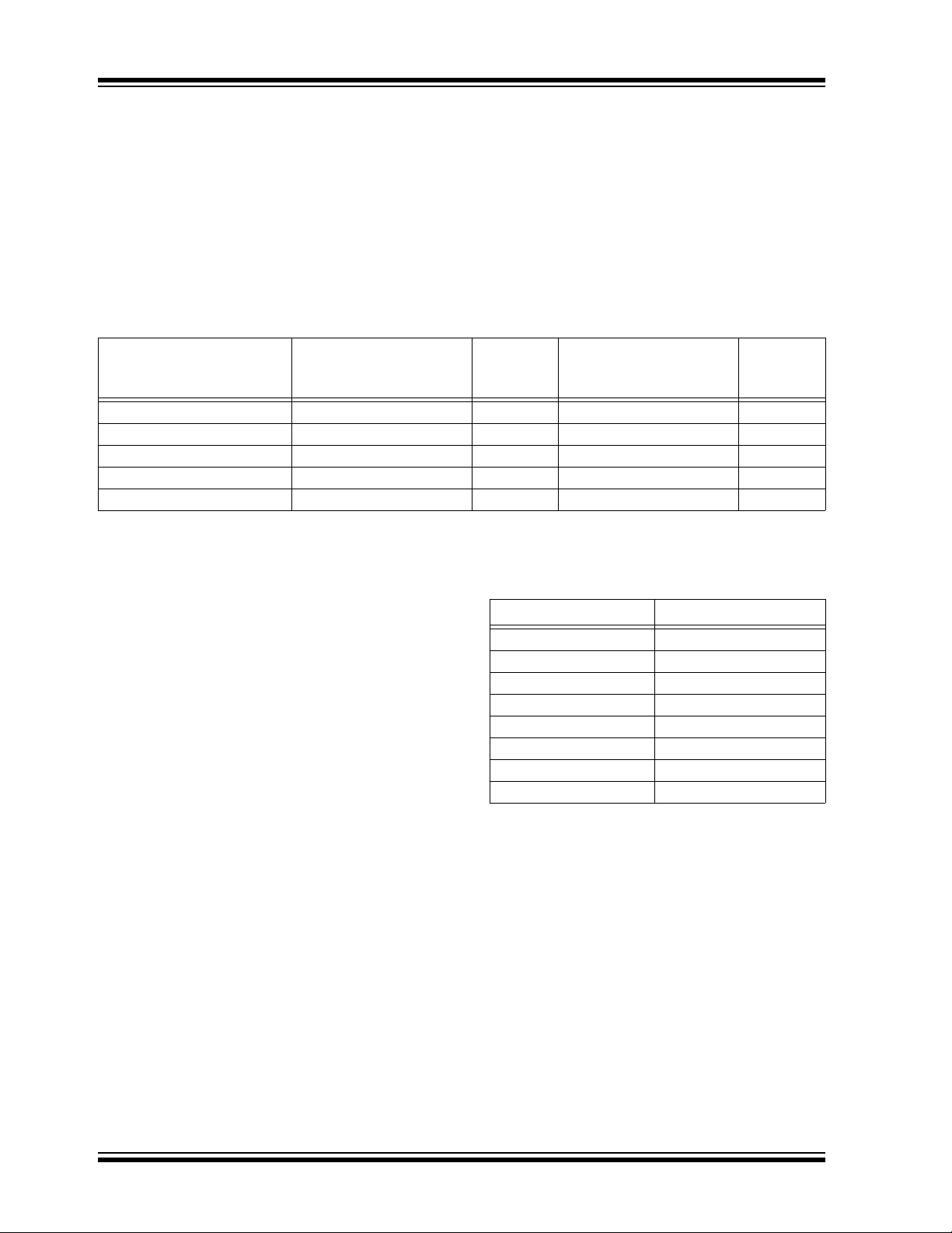
TABLE 2-2: MEMORY SIZES FOR PIC24FXXKA1XX/FVXXKA3XX DEVICES
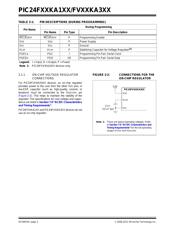
Locations, 800000h through 8007FEh, are reserved for
executive code memory. This region stores the Pro-
gramming Executive, the debugging executive and the
Diagnostic Words. The Programming Executive is used
for device programming and the debug executive is
used for in-circuit debugging. This region of memory
cannot be used to store user code.
The device Configuration registers are implemented
from location, F80000h to F80010h, and can be erased
or programmed one register at a time. Table 2-3 pro-
vides the implemented Configuration registers and
their locations.
Locations, FF0000h and FF0002h, are reserved for the
Device ID registers. These bits can be used by the
programmer to identify the device type that is being
programmed. See Section 6.0 “Device ID” for more
information. The Device ID registers read out normally,
even after code protection is applied.
Figure 2-4 depicts the memory map for the
PIC24FXXKA1XX/FVXXKA3XX family variants.
TABLE 2-3: CONFIGURATION REGISTER
LOCATIONS
Device
Program Memory
Upper Address
(Instruction Words)
Rows
Data EEPROM Size
(Words)
Rows
PIC24F08KA10X 15FEh (2.75K) 88 256 32
PIC24F16KA10X 2BFEh (5.5K) 176 256 32
PIC24FV08KA30X
(1)
15FEh (2.75K) 88 256 32
PIC24FV16KA30X
(1)
2BFEh (5.5K) 176 256 32
PIC24FV32KA30X
(1)
57FEh (11K) 352 256 32
Note 1: This includes corresponding PIC24FXXKA3XX devices.
Configuration Register Address
FBS F80000
FGS F80004
FOSCSEL F80006
FOSC F80008
FWDT F8000A
FPOR F8000C
FICD F8000E
FDS F80010
器件 Datasheet 文档搜索
AiEMA 数据库涵盖高达 72,405,303 个元件的数据手册,每天更新 5,000 多个 PDF 文件
