Datasheet 搜索 > 微控制器 > Microchip(微芯) > PIC24FJ256DA206-I/MR 数据手册 > PIC24FJ256DA206-I/MR 用户编程技术手册 2/48 页
 器件3D模型
¥ 8.685
PIC24FJ256DA206-I/MR 用户编程技术手册 - Microchip(微芯)
制造商:
Microchip(微芯)
分类:
微控制器
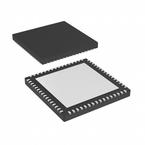
封装:
QFN-64
描述:
PIC24FJ256 系列 16位 96 KB Ram 256 kB 闪存 表面贴装 微控制器 - QFN-64
Pictures:
3D模型
符号图
焊盘图
引脚图
产品图
页面导航:
引脚图在P2P3Hot
导航目录
PIC24FJ256DA206-I/MR数据手册
Page:
of 48 Go
若手册格式错乱,请下载阅览PDF原文件
PIC24FJXXXDA1/DA2/GB2
DS39970A-page 2 2010 Microchip Technology Inc.
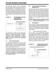
The Enhanced In-Circuit Serial Programming
(Enhanced ICSP) protocol uses a faster method that
takes advantage of the programming executive, as
illustrated in Figure 2-1. The programming executive
provides all the necessary functionality to erase, pro-
gram and verify the chip through a small command set.
The command set allows the programmer to program
the PIC24FJXXXDA1/DA2/GB2 MCUs without having
to deal with the low-level programming protocols of the
chip.
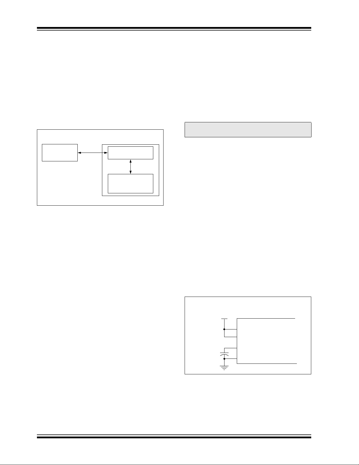
FIGURE 2-1: PROGRAMMING SYSTEM
OVERVIEW FOR
ENHANCED ICSP™
This specification is divided into major sections that
describe the programming methods independently.
Section 3.0 “Device Programming – ICSP™”
describes the In-Circuit Serial Programming method.
Section 4.0 “Device Programming – Enhanced
ICSP™” describes the Run-Time Self-Programming
(RTSP) method.
2.1 Power Requirements
All PIC24FJXXXDA1/DA2/GB2 devices power their
core digital logic at a nominal 1.8V. To simplify system
design, all devices in the PIC24FJXXXDA1/DA2/GB2
families incorporate an on-chip regulator that allows the
device to run its core logic from VDD.
The regulator provides power to the core from the other
V
DD pins. A low-ESR capacitor (such as ceramic or tan-
talum) must be connected to the V
CAP pin (see Table 2-1
and Figure 2-2). This helps to maintain the stability of the
regulator. The specifications for core voltage and capac-
itance are listed in Section 7.0 “AC/DC Characteristics
and Timing Requirements”.
2.2 Program Memory Write/Erase
Requirements
The Flash program memory on PIC24FJXXXDA1/DA2/
GB2 devices has a specific write/erase requirement
that must be adhered to for proper device operation.
The rule is that, any given word in memory must not be
written more than twice before erasing the page in
which it is located. Thus, the easiest way to conform to
this rule is to write all the data in a programming block
within one write cycle. The programming methods
specified in this specification comply with this
requirement.
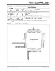
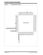
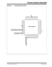
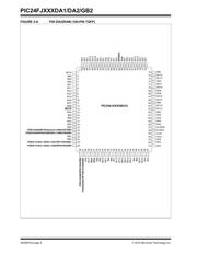
2.3 Pin Diagrams
Figure 2-3, Figure 2-4, Figure 2-5 and Figure 2-6 provide
the pin diagrams for the PIC24FJXXXDA1/DA2/GB2 fam-
ilies. The pins that are required for programming are listed
in Table 2-1 and are indicated in bold text in the figures.
Refer to the appropriate device data sheet for complete
pin descriptions.
2.3.1 PGECx AND PGEDx PIN PAIRS
All of the devices in the PIC24FJXXXDA1/DA2/GB2
families have three separate pairs of programming
pins, labelled as PGEC1/PGED1, PGEC2/PGED2 and
PGEC3/PGED3. Any one of these pin pairs may be
used for device programming by either ICSP or
Enhanced ICSP. Unlike voltage supply and ground
pins, it is not necessary to connect all three pin pairs to
program the device. However, the programming
method must use both pins of the same pair.
FIGURE 2-2: CONNECTIONS FOR THE
ON-CHIP REGULATOR
PIC24FJXXXDA1/DA2/GB2
Programmer
Programming
Executive
On-Chip Memory
Note: Writing to a location multiple times without
erasing is not recommended.
VDD
ENVREG
V
CAP
VSS
PIC24FJXXXDA1/DA2/GB2
CEFC
3.3V
Regulator Enabled (ENVREG tied to VDD):
(10
F typ)
器件 Datasheet 文档搜索
AiEMA 数据库涵盖高达 72,405,303 个元件的数据手册,每天更新 5,000 多个 PDF 文件
