Datasheet 搜索 > 微控制器 > Microchip(微芯) > PIC24FV32KA302-I/SP 数据手册 > PIC24FV32KA302-I/SP 用户编程技术手册 6/54 页
 器件3D模型
¥ 4.284
PIC24FV32KA302-I/SP 用户编程技术手册 - Microchip(微芯)
制造商:
Microchip(微芯)
分类:
微控制器
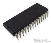
封装:
DIP-28
描述:
MICROCHIP PIC24FV32KA302-I/SP 微控制器, 16位, 通用, PIC24FV, 32 MHz, 32 KB, 2 KB, 28 引脚, SDIP
Pictures:
3D模型
符号图
焊盘图
引脚图
产品图
页面导航:
引脚图在P2P3Hot
技术参数、封装参数在P1
导航目录
PIC24FV32KA302-I/SP数据手册
Page:
of 54 Go
若手册格式错乱,请下载阅览PDF原文件
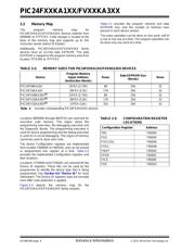
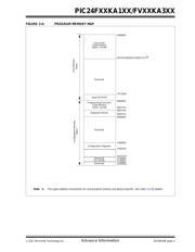
PIC24FXXKA1XX/FVXXKA3XX
DS39919B-page 6 Advance Information 2011 Microchip Technology Inc.
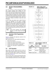
3.0 DEVICE PROGRAMMING –
ICSP
The ICSP method is a special programming protocol
that allows reading and writing to the
PIC24FXXKA1XX/FVXXKA3XX device family memory.
ICSP is the most direct method used to program a
device; however, Enhanced ICSP is faster. The ICSP
mode also reads the contents of the executive memory
to determine if the programming executive is present.
This is accomplished by applying control codes and
instructions, serially to the device, using PGCx and
PGDx pins.
In ICSP mode, the system clock is taken from the
PGCx pin regardless of the device‘s oscillator
Configuration bits. All of the instructions are shifted
serially to an internal buffer, loaded into the Instruction
Register (IR), and then executed. No program is
fetched from the internal memory. Instructions are fed
in 24 bits at a time. PGDx is used to shift data in, and
PGCx is used as both the serial shift clock and the CPU
execution clock.
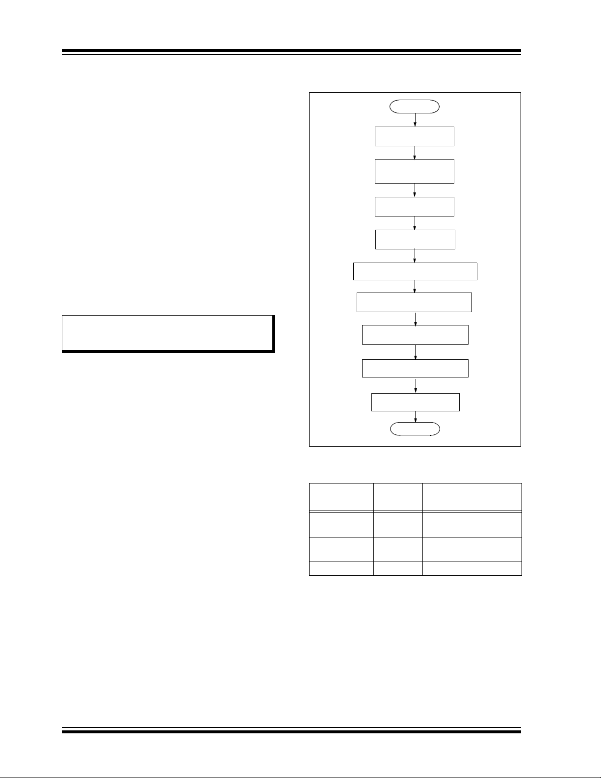
3.1 Overview of the Programming
Process
Figure 3-1 illustrates the high-level overview of the
programming process.
After entering the ICSP mode, perform the following:
1. Bulk Erase the device.
2. Program and verify the code memory.
3. Program and verify the data EEPROM memory.
4. Program and verify the device configuration.
5. Program the code-protect Configuration bits, if
required.
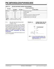
3.2 ICSP Operation
Upon entry into ICSP mode, the CPU is Idle. An
internal state machine governs the execution of the
CPU. A 4-bit control code is clocked in, using PGCx
and PGDx, and this control code is used to command
the CPU (see Table 3-1).
The SIX control code is used to send instructions to the
CPU for execution, and the REGOUT control code is
used to read data out of the device via the VISI register.
FIGURE 3-1: HIGH–LEVEL ICSP™
PROGRAMMING FLOW
TABLE 3-1: CPU CONTROL CODES IN
ICSP™ MODE
Note: During ICSP operation, the operating
frequency of PGCx should not exceed
8 MHz.
4-Bit
Control Code
Mnemonic Description
0000b SIX Shift in 24-bit instruction
and execute.
0001b REGOUT Shift out the VISI
(0784h) register.
0010b-1111b N/A This is reserved.
Start
Perform Bulk
Erase
Program Memory
Verify Program
End
Enter ICSP™ Mode
Program Configuration Bits
Verify Configuration Bits
Exit ICSP Mode
Program Data EEPROM Memory
Verify Data EEPROM Memory
器件 Datasheet 文档搜索
AiEMA 数据库涵盖高达 72,405,303 个元件的数据手册,每天更新 5,000 多个 PDF 文件
