Datasheet 搜索 > 开发套件 > TI(德州仪器) > TPS74401EVM-118 数据手册 > TPS74401EVM-118 用户编程技术手册 6/40 页

¥ 89.003
TPS74401EVM-118 用户编程技术手册 - TI(德州仪器)
制造商:
TI(德州仪器)
分类:
开发套件
封装:
-
描述:
TEXAS INSTRUMENTS TPS74401EVM-118 评估模块, TPS74401EVM-118
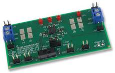
Pictures:
3D模型
符号图
焊盘图
引脚图
产品图
页面导航:
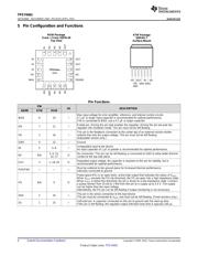
引脚图在P4Hot
典型应用电路图在P1P20P24P25
原理图在P13P14P24P25P26
封装尺寸在P31P33P34
标记信息在P31P32
封装信息在P30P31P32P33P34
技术参数、封装参数在P5
应用领域在P1P20P32P40
电气规格在P6P7
导航目录
TPS74401EVM-118数据手册
Page:
of 40 Go
若手册格式错乱,请下载阅览PDF原文件
TPS74401
SBVS066Q –DECEMBER 2005–REVISED APRIL 2015
www.ti.com
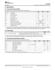
6.4 Thermal Information
TPS74401
(3)
THERMAL METRIC
(1)(2)
RGW (VQFN) KTW (DDPAK) UNIT
20 PINS 7 PINS
R
θJA
Junction-to-ambient thermal resistance 35.4 26.6
R
θJC(top)
Junction-to-case (top) thermal resistance 32.4 41.7
R
θJB
Junction-to-board thermal resistance 14.7 12.5
°C/W
ψ
JT
Junction-to-top characterization parameter 0.4 4.0
ψ
JB
Junction-to-board characterization parameter 14.8 7.3
R
θJC(bot)
Junction-to-case (bottom) thermal resistance 3.9 0.3
(1) For more information about traditional and new thermal metrics, see the IC Package Thermal Metrics application report, SPRA953.
(2) For thermal estimates of this device based on PCB copper area, see the TI PCB Thermal Calculator.
(3) Thermal data for the RGW and KTW packages are derived by thermal simulations based on JEDEC-standard methodology as specified
in the JESD51 series. The following assumptions are used in the simulations:
(a) i. RGW: The exposed pad is connected to the PCB ground layer through a 4x4 thermal via array.
- ii. KTW: The exposed pad is connected to the PCB ground layer through a 6x6 thermal via array.
(b) Each of top and bottom copper layers has a dedicated pattern for 20% copper coverage.
(c) These data were generated with only a single device at the center of a JEDEC high-K (2s2p) board with 3in × 3in copper area. To
understand the effects of the copper area on thermal performance, refer to the Thermal Considerations section.
6.5 Electrical Characteristics
At V
EN
= 1.1 V, V
IN
= V
OUT
+ 0.3 V, C
IN
= C
BIAS
= 0.1 μF, C
OUT
= 10 μF, I
OUT
= 50 mA, V
BIAS
= 5.0 V, and T
J
= –40°C to 125°C,
unless otherwise noted. Typical values are at T
J
= 25°C.
PARAMETER TEST CONDITIONS MIN TYP MAX UNIT
V
IN
Input voltage range V
OUT
+ V
DO
5.5 V
V
BIAS
Bias pin voltage range 2.375 5.25 V
Internal reference
V
REF
T
J
= 25°C 0.796 0.8 0.804 V
(adjustable version)
Output voltage range V
IN
= 5 V, I
OUT
= 1.5 A, V
BIAS
= 5 V V
REF
3.6 V
2.97 V ≤ V
BIAS
≤ 5.25 V, V
OUT
+ 1.62 V ≤ V
BIAS
,
–1% ±0.2% 1%
V
OUT
50 mA ≤ I
OUT
≤ 3.0 A
(1)
Accuracy
V
OUT
+ V
DO
BIAS ≤ V
BIAS
≤ 5.25 V,
–1% ±0.2% 1%
100 mA ≤ I
OUT
≤ I
VDO BIAS
, VQFN
(2)
V
OUT(nom)
+ 0.3 ≤ V
IN
≤ 5.5 V, VQFN 0.0005 0.05 %/V
ΔV
OUT(ΔVIN)
Line regulation
V
OUT(nom)
+ 0.3 ≤ V
IN
≤ 5.5 V, DDPAK 0.0005 0.06 %/V
0 mA ≤ I
OUT
≤ 50 mA 0.013 %/mA
ΔV
OUT(ΔIOUT)
Load regulation
50 mA ≤ I
OUT
≤ 3.0 A 0.03 %/A
I
OUT
= 3.0 A, V
BIAS
– V
OUT(nom)
≥ 1.62 V, VQFN 115 195 mV
V
IN
dropout voltage
(3)
I
OUT
= 3.0 A, V
BIAS
– V
OUT(nom)
≥ 1.62 V, DDPAK 120 240 mV
I
OUT
= 3.0 A, V
IN
= V
BIAS
1.62 V
V
DO
I
OUT
= 3.0 A 1.62 V
V
BIAS
dropout voltage
(3)
I
OUT
= 1.0 A 1.35 V
I
OUT
= 500 mA 1.27 V
I
OUT
= 100 mA 1.16 V
V
OUT
= 80% × V
OUT(nom)
, VQFN 3.8 6.0 A
I
CL
Current limit
V
OUT
= 80% × V
OUT(nom)
, DDPAK 3.5 6.0 A
I
BIAS
Bias pin current I
OUT
= 0 mA to 3.0 A 2 4 mA
I
SHDN
Shutdown supply current (V
IN
) V
EN
≤ 0.4 V 1 100 μA
I
FB
, I
SNS
Feedback, sense pin current
(4)
I
OUT
= 50 mA to 3.0 A –250 95 250 nA
(1) Adjustable devices tested at 0.8 V; external resistor tolerance is not taken into account.
(2) V
OUT
is set to 1.5 V to avoid minimum V
BIAS
restrictions.
(3) Dropout is defined as the voltage from the input to V
OUT
when V
OUT
is 2% below nominal.
(4) I
FB
, I
SNS
current flow is out of the device.
6 Submit Documentation Feedback Copyright © 2005–2015, Texas Instruments Incorporated
Product Folder Links: TPS74401
器件 Datasheet 文档搜索
AiEMA 数据库涵盖高达 72,405,303 个元件的数据手册,每天更新 5,000 多个 PDF 文件
