Datasheet 搜索 > SCSI控制器 > TI(德州仪器) > UCC5614PWPG4 数据手册 > UCC5614PWPG4 用户编程技术手册 1/16 页
 器件3D模型
¥ 35.181
UCC5614PWPG4 用户编程技术手册 - TI(德州仪器)
制造商:
TI(德州仪器)
分类:
SCSI控制器
封装:
TSSOP-24
描述:
SCSI 接口集成电路 Lowest Capacitance 9-Line 3-5V SE
Pictures:
3D模型
符号图
焊盘图
引脚图
产品图
页面导航:
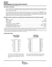
封装尺寸在P9P11P12
标记信息在P9P10
封装信息在P1P9P10P11P12
导航目录
UCC5614PWPG4数据手册
Page:
of 16 Go
若手册格式错乱,请下载阅览PDF原文件
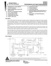
SLUS241D − MARCH 1994 - REVISED NOVEMBER 2003
1
www.ti.com
D Integrated 0.15-Ω Power MOSFET
D 3-V to 8-V Operation
D Digital Programmable Current Limit
from 0 A to 3 A
D Electronic Circuit Breaker Function
D 1µA I
CC
When Disabled
D Programmable On-Time
D Programmable Start Delay
D Fixed 3% Duty Cycle
D Unidirectional Switch
D Thermal Shutdown
D Fault-Output Indicator
D Maximum-Output Current Can Be Set to 1 A
Above the Programmed Fault Level or to a
Full 4 A
D Power SOIC, Low-Thermal Resistance
Packaging
description
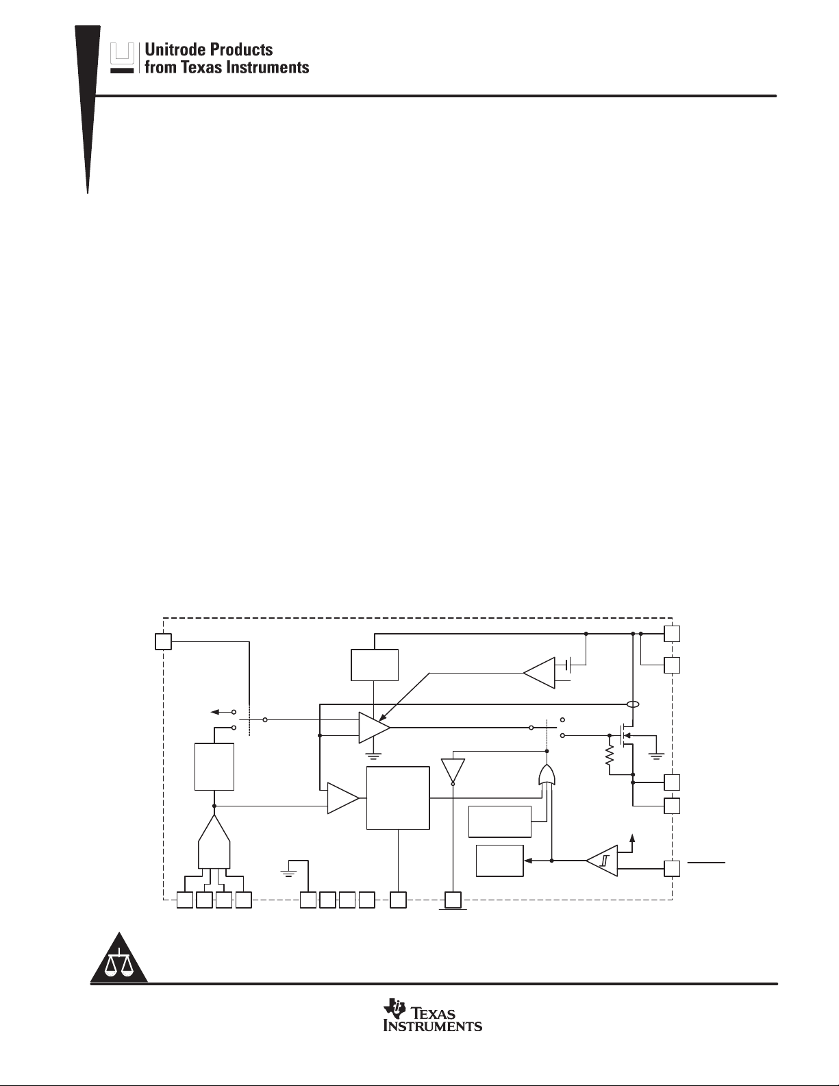
The UCC3912 family of hot swap power managers provides complete power management, hot swap capability,
and circuit breaker functions. The only component required to operate the device, other than supply bypassing,
is the fault timing capacitor, C
T
. All control and housekeeping functions are integrated, and externally
programmable. These include the fault current level, maximum output-sourcing current, maximum fault time,
and startup delay. In the event of a constant fault, the internal fixed 3% duty cycle ratio limits average output
power.
The internal 4-bit DAC allows programming of the fault level current from 0 A to 3 A with 0.25-A resolution. The
IMAX control pin sets the maximum sourcing current to 1 A above the fault level when driven low, and to a full
4 A when driven high for applications which require fast output capacitor charging.
When the output current is below the fault level, the output MOSFET is switched on with a nominal on resistance
of 0.15 Ω. When the output current exceeds the fault level, but is less than the maximum sourcing level, the
output remains switched on, but the fault timer starts charging C
T
. Once C
T
charges to a preset threshold, the
switch is turned off, and remains off for 30 times the programmed fault time. When the output current reaches
the maximum sourcing level, the MOSFET transitions from a switch to a constant current source. (continued)
block diagram
UDG-99146
B1 B0
6 7 8
2
3
9 11 16
0 A−3 A
0.25
RES
B3 B2
5 4 13 12
CT
ON TIME
CONTROL
3% DUTY
CYCLE
+
−
THERMAL
SHUTDOWN
INTERNAL
BIAS
+
−
1
SHTDWN
14
15
1.5 V
H = OPEN
FAULT
CURRENT SENSE
+
−
+
CHARGE
PUMP
30 mV
V
OUT
REVERSE VOLTAGE
COMPARATOR
+
−
LINEAR CURRENT AMPLIFIER
1 A
ABOVE
FAULT
10IMAX
GND
HEATSINK
GND PINS
CURRENT FAULT
LEVEL 0A TO 3 A
OVERCURRENT
COMPARATOR
MAX CURRENT
LEVEL
4 A
H = 4 A VIN
VIN
VOUT
VOUT
POWER
FET
4 BIT DAC
Copyright 2003, Texas Instruments Incorporated
! "#$ ! %#&'" ($)
(#"! " !%$""! %$ *$ $! $+! !#$!
!(( ,-) (#" %"$!!. ($! $"$!!'- "'#($
$!. '' %$$!)
Please be aware that an important notice concerning availability, standard warranty, and use in critical applications of
Texas Instruments semiconductor products and disclaimers thereto appears at the end of this data sheet.
器件 Datasheet 文档搜索
AiEMA 数据库涵盖高达 72,405,303 个元件的数据手册,每天更新 5,000 多个 PDF 文件
