Datasheet 搜索 > EEPROM芯片 > Xilinx(赛灵思) > XC18V02VQ44C 数据手册 > XC18V02VQ44C 用户编程技术手册 2/25 页
 器件3D模型
¥ 112.93
XC18V02VQ44C 用户编程技术手册 - Xilinx(赛灵思)
制造商:
Xilinx(赛灵思)
分类:
EEPROM芯片
封装:
TQFP-44
描述:
XC18V02VQ44C 磨码
Pictures:
3D模型
符号图
焊盘图
引脚图
产品图
页面导航:

导航目录
XC18V02VQ44C数据手册
Page:
of 25 Go
若手册格式错乱,请下载阅览PDF原文件
XC18V00 Series In-System-Programmable Configuration PROMs
DS026 (v6.0) August 5, 2015 www.xilinx.com
Product Specification 2
R
— PRODUCT OBSOLETE / UNDER OBSOLESCENCE —
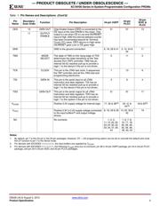
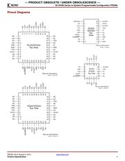
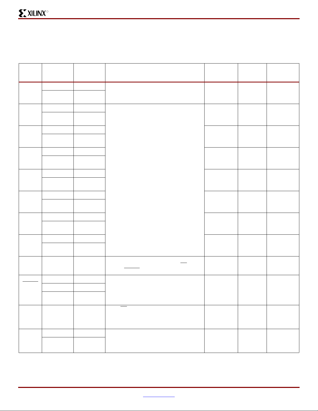
Pinout and Pin Description
Table 1 provides a list of the pin names and descriptions for the 44-pin VQFP and PLCC and the 20-pin SOIC and PLCC
packages.
Table 1: Pin Names and Descriptions
Pin
Name
Boundary-
Scan Order
Function Pin Description 44-pin VQFP
44-pin
PLCC
20-pin
SOIC &
PLCC
D0 4 DATA OUT D0 is the DATA output pin to provide data for
configuring an FPGA in serial mode.
40 2 1
3OUTPUT
ENABLE
D1 6 DATA OUT D0-D7 are the output pins to provide parallel
data for configuring a Xilinx FPGA in Slave
Parallel/SelectMAP mode.
D1-D7 remain in high-Z state when the PROM
operates in serial mode.
D1-D7 can be left unconnected when the
PROM is used in serial mode.
29 35 16
5OUTPUT
ENABLE
D2 2 DATA OUT 42 4 2
1OUTPUT
ENABLE
D3 8 DATA OUT 27 33 15
7OUTPUT
ENABLE
D4 24 DATA OUT 9 15 7
(1)
23 OUTPUT
ENABLE
D5 10 DATA OUT 25 31 14
9OUTPUT
ENABLE
D6 17 DATA OUT 14 20 9
16 OUTPUT
ENABLE
D7 14 DATA OUT 19 25 12
13 OUTPUT
ENABLE
CLK 0 DATA IN Each rising edge on the CLK input increments
the internal address counter if both CE
is Low
and OE/RESET
is High.
43 5 3
OE/
RESET
20 DATA IN When Low, this input holds the address
counter reset and the DATA output is in a high-
Z state. This is a bidirectional open-drain pin
that is held Low while the PROM is reset.
Polarity is NOT programmable.
13 19 8
19 DATA OUT
18 OUTPUT
ENABLE
CE 15 DATA IN When CE
is High, the device is put into low-
power standby mode, the address counter is
reset, and the DATA pins are put in a high-Z
state.
15 21 10
CF 22 DATA OUT Allows JTAG CONFIG instruction to initiate
FPGA configuration without powering down
FPGA. This is an open-drain output that is
pulsed Low by the JTAG CONFIG command.
10 16 7
(1)
21 OUTPUT
ENABLE
器件 Datasheet 文档搜索
AiEMA 数据库涵盖高达 72,405,303 个元件的数据手册,每天更新 5,000 多个 PDF 文件
