Datasheet 搜索 > EEPROM芯片 > Xilinx(赛灵思) > XC18V04VQ44C 数据手册 > XC18V04VQ44C 用户编程技术手册 6/25 页
 器件3D模型
¥ 12.941
XC18V04VQ44C 用户编程技术手册 - Xilinx(赛灵思)
制造商:
Xilinx(赛灵思)
分类:
EEPROM芯片
封装:
TQFP-44
描述:
XC18V04VQ44C 磨码
Pictures:
3D模型
符号图
焊盘图
引脚图
产品图
页面导航:

导航目录
XC18V04VQ44C数据手册
Page:
of 25 Go
若手册格式错乱,请下载阅览PDF原文件
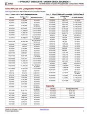
XC18V00 Series In-System-Programmable Configuration PROMs
DS026 (v6.0) August 5, 2015 www.xilinx.com
Product Specification 6
R
— PRODUCT OBSOLETE / UNDER OBSOLESCENCE —
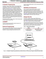
In-System Programming
In-System Programmable PROMs can be programmed
individually, or two or more can be chained together and
programmed in-system via the standard 4-pin JTAG
protocol as shown in Figure 2. In-system programming
offers quick and efficient design iterations and eliminates
unnecessary package handling or socketing of devices. The
Xilinx development system provides the programming data
sequence using either Xilinx iMPACT software and a
download cable, a third-party JTAG development system, a
JTAG-compatible board tester, or a simple microprocessor
interface that emulates the JTAG instruction sequence. The
iMPACT software also outputs serial vector format (SVF)
files for use with any tools that accept SVF format and with
automatic test equipment.
All outputs are held in a high-Z state or held at clamp levels
during in-system programming.
OE/RESET
The ISP programming algorithm requires issuance of a
reset that causes OE to go Low.
External Programming
Xilinx reprogrammable PROMs can also be programmed by
a third-party device programmer, providing the added
flexibility of using pre-programmed devices with an in-
system programmable option for future enhancements and
design changes.
Reliability and Endurance
Xilinx in-system programmable products provide a
guaranteed endurance level of 20,000 in-system
program/erase cycles and a minimum data retention of 20
years. Each device meets all functional, performance, and
data retention specifications within this endurance limit. See
the UG116
, Xilinx Device Reliability Report, for device
quality, reliability, and process node information.
Design Security
The Xilinx in-system programmable PROM devices
incorporate advanced data security features to fully protect
the programming data against unauthorized reading via
JTAG. Table 3 shows the security setting available.
The read security bit can be set by the user to prevent the
internal programming pattern from being read or copied via
JTAG. When set, it allows device erase. Erasing the entire
device is the only way to reset the read security bit.
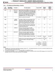
Tabl e 3 : Data Security Options
Reset Set
Read Allowed
Program/Erase Allowed
Verify Allowed
Read Inhibited via JTAG
Program/Erase Allowed
Verify Inhibited
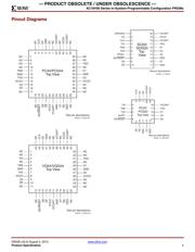
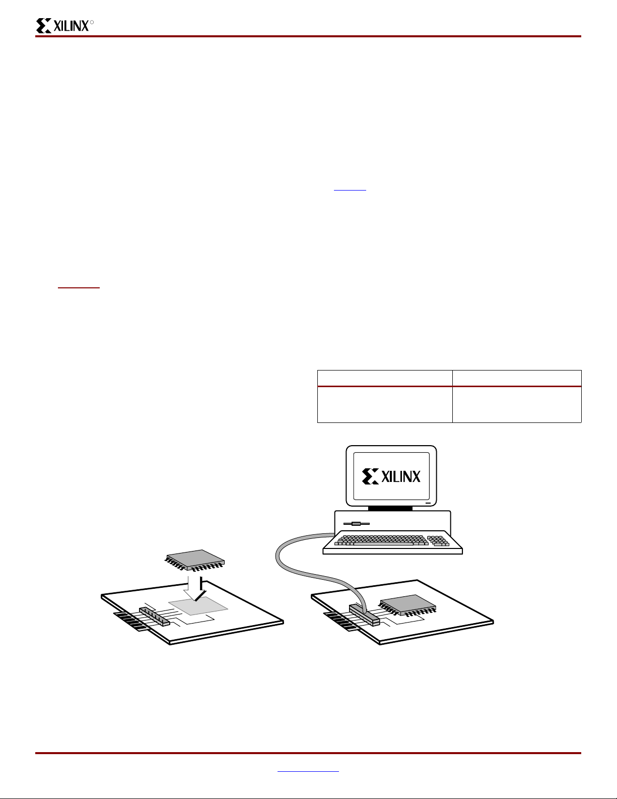
X-Ref Target - Figure 2
Figure 2: In-System Programming Operation (a) Solder Device to PCB and (b) Program Using Download Cable
DS026_02_06/1103
GND
V
CCINT
(a) (b)
器件 Datasheet 文档搜索
AiEMA 数据库涵盖高达 72,405,303 个元件的数据手册,每天更新 5,000 多个 PDF 文件
