Datasheet 搜索 > FPGA芯片 > Xilinx(赛灵思) > XC4010E-4PC84I 数据手册 > XC4010E-4PC84I 用户编程技术手册 1/68 页
 器件3D模型
¥ 73.704
XC4010E-4PC84I 用户编程技术手册 - Xilinx(赛灵思)
制造商:
Xilinx(赛灵思)
分类:
FPGA芯片
封装:
PLCC-84
Pictures:
3D模型
符号图
焊盘图
引脚图
产品图
页面导航:
导航目录
XC4010E-4PC84I数据手册
Page:
of 68 Go
若手册格式错乱,请下载阅览PDF原文件
May 14, 1999 (Version 1.6) 6-5
6
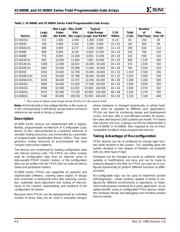
XC4000E and XC4000X Series
Features
Note: Information in this data sheet covers the XC4000E,
XC4000EX, and XC4000XL families.Aseparatedatasheet
covers the XC4000XLA and XC4000XV families. Electrical
Specifications and package/pin information are covered in
separate sections for each family to make the information
easier to access,review, and print. For access to thesesec-
tions, see the Xilinx WEBLINX web site at
http://www.xilinx.com/partinfo/databook.htm#xc4000.
• System featured Field-Programmable Gate Arrays
- Select-RAM
TM
memory: on-chip ultra-fast RAM with
- synchronous write option
- dual-port RAM option
- Fully PCI compliant (speed grades -2 and faster)
- Abundant flip-flops
- Flexible function generators
- Dedicated high-speed carry logic
- Wide edge decoders on each edge
- Hierarchy of interconnect lines
- Internal 3-state bus capability
- Eight global low-skew clock or signal distribution
networks
• System Performance beyond 80 MHz
• Flexible Array Architecture
• Low Power Segmented Routing Architecture
• Systems-Oriented Features
- IEEE 1149.1-compatible boundary scan logic
support
- Individually programmable output slew rate
- Programmable input pull-up or pull-down resistors
- 12 mA sink current per XC4000E output
• Configured by Loading Binary File
- Unlimited re-programmability
• Read Back Capability
- Program verification
- Internal node observability
• Backward Compatible with XC4000 Devices
• Development System runs on most common computer
platforms
- Interfaces to popular design environments
- Fully automatic mapping, placement and routing
- Interactive design editor for design optimization
Low-Voltage Versions Available
• Low-Voltage Devices Function at 3.0 - 3.6 Volts
• XC4000XL: High Performance Low-Voltage Versions of
XC4000EX devices
Additional XC4000X Series Features
• Highest Performance — 3.3 V XC4000XL
• Highest Capacity — Over 180,000 Usable Gates
• 5 V tolerant I/Os on XC4000XL
• 0.35 µm SRAM process for XC4000XL
• Additional Routing Over XC4000E
- almost twice the routing capacity for high-density
designs
• Buffered Interconnect for Maximum Speed Blocks
• Improved VersaRing
TM
I/O Interconnect for Better Fixed
Pinout Flexibility
• 12 mA Sink Current Per XC4000X Output
• Flexible New High-Speed Clock Network
- Eight additional Early Buffers forshorter clock delays
- Virtually unlimited number of clock signals
• Optional Multiplexer or 2-input Function Generator on
Device Outputs
• Four Additional Address Bits in Master Parallel
Configuration Mode
• XC4000XV Family offers the highest density with
0.25 µm 2.5 V technology
Introduction
XC4000 Series high-performance, high-capacity Field Pro-
grammable Gate Arrays (FPGAs) provide the benefits of
custom CMOS VLSI, while avoiding the initial cost, long
development cycle, and inherent risk of a conventional
masked gate array.
The result of thirteen yearsofFPGAdesignexperience and
feedback from thousands of customers, these FPGAs com-
bine architectural versatility, on-chip Select-RAM memory
with edge-triggered and dual-port modes, increased
speed, abundant routing resources, and new, sophisticated
software to achieve fully automated implementation of
complex, high-density, high-performance designs.
The XC4000E and XC4000X Series currently have 20
members, as shown in Table 1.
0
XC4000E and XC4000X Series Field
Programmable Gate Arrays
May 14, 1999 (Version 1.6)
00*
Product Specification
R
器件 Datasheet 文档搜索
AiEMA 数据库涵盖高达 72,405,303 个元件的数据手册,每天更新 5,000 多个 PDF 文件
