Datasheet 搜索 > 微处理器 > Xilinx(赛灵思) > XC7Z030-2FFG676I 数据手册 > XC7Z030-2FFG676I 用户编程技术手册 2/85 页
 器件3D模型
¥ 340.356
XC7Z030-2FFG676I 用户编程技术手册 - Xilinx(赛灵思)
制造商:
Xilinx(赛灵思)
分类:
微处理器
封装:
BBGA-676
描述:
PSoC/MPSoC微处理器, Zynq-7000 XC7Z030系列, ARM Cortex-A9,800 MHz, FCBGA-676
Pictures:
3D模型
符号图
焊盘图
引脚图
产品图
页面导航:
封装信息在P2P65
技术参数、封装参数在P1P2P14P71P72P81P82
应用领域在P35P85
电气规格在P17P35
导航目录
XC7Z030-2FFG676I数据手册
Page:
of 85 Go
若手册格式错乱,请下载阅览PDF原文件
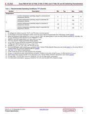
Zynq-7000 AP SoC (Z-7030, Z-7035, Z-7045, and Z-7100): DC and AC Switching Characteristics
DS191 (v1.17) November 24, 2015 www.xilinx.com
Product Specification 2
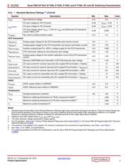
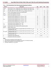
V
REF
Input reference voltage
–0.5 2.0 V
V
IN
(3)(4)(5)
I/O input voltage for HR I/O banks –0.40 V
CCO
+0.55 V
I/O input voltage for HP I/O banks –0.55 V
CCO
+0.55 V
I/O input voltage (when V
CCO
= 3.3V) for V
REF
and differential I/O standards
except TMDS_33
(6)
–0.40 2.625 V
V
CCBATT
Key memory battery backup supply
–0.5 2.0 V
GTX Transceiver
V
MGTAVCC
Analog supply voltage for the GTX transmitter and receiver circuits –0.5 1.1 V
V
MGTAVTT
Analog supply voltage for the GTX transmitter and receiver termination circuits –0.5 1.32 V
V
MGTVCCAUX
Auxiliary analog Quad PLL (QPLL) voltage supply for the GTX transceivers –0.5 1.935 V
V
MGTREFCLK
GTX transceiver reference clock absolute input voltage –0.5 1.32 V
V
MGTAVTTRCAL
Analog supply voltage for the resistor calibration circuit of the GTX transceiver
column
–0.5 1.32 V
V
IN
Receiver (RXP/RXN) and Transmitter (TXP/TXN) absolute input voltage –0.5 1.26 V
I
DCIN-FLOAT
DC input current for receiver input pins DC coupled RX termination = floating – 14 mA
I
DCIN-MGTAVTT
DC input current for receiver input pins DC coupled RX termination = V
MGTAVTT
–12mA
I
DCIN-GND
DC input current for receiver input pins DC coupled RX termination = GND – 6.5 mA
I
DCOUT-FLOAT
DC output current for transmitter pins DC coupled RX termination = floating – 14 mA
I
DCOUT-MGTAVTT
DC output current for transmitter pins DC coupled RX termination = V
MGTAVTT
–12mA
XADC
V
CCADC
XADC supply relative to GNDADC
–0.5 2.0 V
V
REFP
XADC reference input relative to GNDADC
–0.5 2.0 V
Temperature
T
STG
Storage temperature (ambient)
–65 150 °C
T
SOL
Maximum soldering temperature for Pb/Sn component bodies
(7)
– +220 °C
Maximum soldering temperature for Pb-free component bodies
(7)
– +260 °C
T
j
Maximum junction temperature
(7)
– +125 °C
Notes:
1. Stresses beyond those listed under Absolute Maximum Ratings might cause permanent damage to the device. These are stress ratings only,
and functional operation of the device at these or any other conditions beyond those listed under Operating Conditions is not implied.
Exposure to Absolute Maximum Ratings conditions for extended periods of time might affect device reliability.
2. Applies to both MIO supply banks V
CCO_MIO0
and V
CCO_MIO1
.
3. The lower absolute voltage specification always applies.
4. For I/O operation, refer to the 7 Series FPGAs SelectIO Resources User Guide (UG471
) or the Zynq-7000 All Programmable SoC Technical
Reference Manual (UG585
).
5. The maximum limit applies to DC signals. For maximum undershoot and overshoot AC specifications, see Tabl e 4 and Table 5 .
6. See Table 1 2 for TMDS_33 specifications.
7. For soldering guidelines and thermal considerations, see the Zynq-7000 All Programmable SoC Packaging and Pinout Specification
(UG865
).
Tabl e 1: Absolute Maximum Ratings
(1)
(Cont’d)
Symbol Description Min Max Units
Send Feedback
器件 Datasheet 文档搜索
AiEMA 数据库涵盖高达 72,405,303 个元件的数据手册,每天更新 5,000 多个 PDF 文件
