Datasheet 搜索 > 主动器件 > Xilinx(赛灵思) > XCF32PV0G48C 数据手册 > XCF32PV0G48C 用户编程技术手册 6/35 页

¥ 229.147
XCF32PV0G48C 用户编程技术手册 - Xilinx(赛灵思)
制造商:
Xilinx(赛灵思)
分类:
主动器件
封装:
TSOP
描述:
XILINX XCF32PV0G48C 芯片
Pictures:
3D模型
符号图
焊盘图
引脚图
产品图
页面导航:
引脚图在P24P25P26P27P28Hot
原理图在P2P34
型号编码规则在P30
标记信息在P30P31P34
封装信息在P13
技术参数、封装参数在P13P24P33P35
应用领域在P35
电气规格在P1P13P16P33


导航目录
XCF32PV0G48C数据手册
Page:
of 35 Go
若手册格式错乱,请下载阅览PDF原文件
Platform Flash In-System Programmable Configuration PROMs
DS123 (v2.17) October 26, 2009 www.xilinx.com
Product Specification 6
R
Boundary-Scan Register
The Boundary-Scan register is used to control and observe
the state of the device pins during the EXTEST,
SAMPLE/PRELOAD, and CLAMP instructions. Each output
pin on the Platform Flash PROM has two register stages which
contribute to the Boundary-Scan register, while each input pin
has only one register stage. The bidirectional pins have a total
of three register stages which contribute to the Boundary-Scan
register. For each output pin, the register stage nearest to TDI
controls and observes the output state, and the second stage
closest to TDO controls and observes the High-Z enable state
of the output pin. For each input pin, a single register stage
controls and observes the input state of the pin. The
bidirectional pin combines the three bits, the input stage bit is
first, followed by the output stage bit and finally the output
enable stage bit. The output enable stage bit is closest to TDO.
See Table 12, page 24 and Table 13, page 26 for the
Boundary-Scan bit order for all connected device pins, or see
the appropriate BSDL file for the complete Boundary-Scan bit
order description under the “attribute
BOUNDARY_REGISTER” section in the BSDL file. The bit
assigned to Boundary-Scan cell 0 is the LSB in the Boundary-
Scan register, and is the register bit closest to TDO.
Identification Registers
IDCODE Register
The IDCODE is a fixed, vendor-assigned value that is used to
electrically identify the manufacturer and type of the device
being addressed. The IDCODE register is 32 bits wide. The
IDCODE register can be shifted out for examination by using
the IDCODE instruction. The IDCODE is available to any
other system component via JTAG. Table 8 lists the IDCODE
register values for the Platform Flash PROMs.
The IDCODE register has the following binary format:
vvvv:ffff:ffff:aaaa:aaaa:cccc:cccc:ccc1
where
v = the die version number
f = the PROM family code
a = the specific Platform Flash PROM product ID
c = the Xilinx manufacturer's ID
The LSB of the IDCODE register is always read as logic 1
as defined by IEEE Std. 1149.1.
USERCODE Register
The USERCODE instruction gives access to a 32-bit user
programmable scratch pad typically used to supply
information about the device's programmed contents. By
using the USERCODE instruction, a user-programmable
identification code can be shifted out for examination. This
code is loaded into the USERCODE register during
programming of the Platform Flash PROM. If the device is
blank or was not loaded during programming, the
USERCODE register contains FFFFFFFFh.
Customer Code Register
For the XCFxxP Platform Flash PROM, in addition to the
USERCODE, a unique 32-byte Customer Code can be
assigned to each design revision enabled for the PROM.
The Customer Code is set during programming, and is
typically used to supply information about the design
revision contents. A private JTAG instruction is required to
read the Customer Code. If the PROM is blank, or the
Customer Code for the selected design revision was not
loaded during programming, or if the particular design
revision is erased, the Customer Code contains all ones.
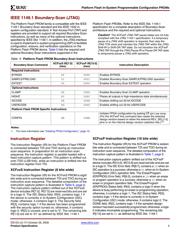
Table 6: XCFxxS Instruction Capture Values Loaded into IR as part of an Instruction Scan Sequence
TDI →
IR[7:5] IR[4] IR[3] IR[2] IR[1:0]
→ TDO
Reserved ISC Status Security 0 0 1
Table 7: XCFxxP Instruction Capture Values Loaded into IR as part of an Instruction Scan Sequence
TDI →
IR[15:9] IR[8:7] IR[6:5] IR[4] IR[3] IR[2] IR[1:0]
→ TDO
Reserved ISC Error
ER/PROG
Error
ER/PROG
Status
ISC Status DONE 0 1
Tabl e 8 : IDCODES Assigned to Platform Flash PROMs
Device IDCODE
(1)
(hex)
XCF01S <v>5044093
XCF02S <v>5045093
XCF04S <v>5046093
XCF08P <v>5057093
XCF16P <v>5058093
XCF32P <v>5059093
Notes:
1. The <v> in the IDCODE field represents the device’s revision
code (in hex) and can vary.
器件 Datasheet 文档搜索
AiEMA 数据库涵盖高达 72,405,303 个元件的数据手册,每天更新 5,000 多个 PDF 文件
