Datasheet 搜索 > 微控制器 > Microchip(微芯) > DSPIC33FJ128GP802-E/MM 数据手册 > DSPIC33FJ128GP802-E/MM 开发手册 1/34 页
 器件3D模型
¥ 50.181
DSPIC33FJ128GP802-E/MM 开发手册 - Microchip(微芯)
制造商:
Microchip(微芯)
分类:
微控制器
封装:
QFN-28
描述:
DSPIC33FJ128GP802-E/MM 管装
Pictures:
3D模型
符号图
焊盘图
引脚图
产品图
页面导航:
原理图在P5
功能描述在P24
导航目录
DSPIC33FJ128GP802-E/MM数据手册
Page:
of 34 Go
若手册格式错乱,请下载阅览PDF原文件
© 2008 Microchip Technology Inc. DS01210A-page 1
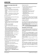
AN1210
INTRODUCTION
This application note describes the methodology to use
the Parallel Master Port (PMP) module to interface with
external data memory; either external Flash or external
RAM. This application note also lists the APIs and
describes how to implement different types of
interfaces.
Using the PMP module, the memory devices with
64K locations (Kbytes or K words) can be interfaced
with no extra I/Os and software. This application note
describes how to interface the memory devices with
more than 64K locations using some I/O pins and
provides the required APIs.
This application note describes the following topics:
• “External Data Memory Interface Overview”
• “Functional Implementation”
• “Expansion Of External Memory”
• “Reference Code”
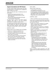
EXTERNAL DATA MEMORY
INTERFACE OVERVIEW
The PIC24F/24H/dsPIC33F architecture supports up to
64 Kbytes of internal data memory. If internal memory
is insufficient, the external memory can be used. But,
this external memory cannot be directly accessed by
the CPU of the controller. The CPU can access through
the PMP module.
This section describes the topics:
• Signals Required for Interfacing Memory Devices
• Signals Generated by the PMP Module
• Registers Associated with the PMP Module
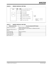
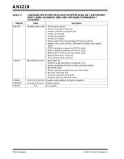
Signals Required for Interfacing Memory
Devices
Table 1 provides the signals required to interface
different types of memory devices.
TABLE 1: TYPICAL MEMORY DEVICE
INTERFACE CONNECTIONS
Author: Vidyadhar Vivekananda
Microchip Technology Inc.
Pin Name Function
Address Lines
(A0toAn)
‘n’ number of lines are
required to address all the
memory locations in a
2
n
Kbytes/K words memory
device.
Data Lines
(I/O 0 to 7 or I/O 0 to
15)
8 or 16 Data Lines are
required to read/write the
data in a byte or word
memory device.
Chip Enable
(CE
)
One Chip Enable signal for
each memory device.
Write Enable
(WE
)
One Write Enable signal,
which should go active
whenever data is to be
written into the memory
device.
Output Enable
(OE
)
One Output Enable signal,
which should go active
whenever data is to be read
from the memory device.
Byte Enable (A-1) and
Word/Byte
One Byte Enable signal and
one Word/Byte
signal, if the
memory device is a 16-bit
device and supports both
Word and Byte modes.
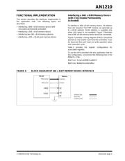
Using External Data Memory with
PIC24F/24H/dsPIC33F Devices
器件 Datasheet 文档搜索
AiEMA 数据库涵盖高达 72,405,303 个元件的数据手册,每天更新 5,000 多个 PDF 文件
