Datasheet 搜索 > 逻辑控制器 > ADI(亚德诺) > ADG901BCPZ-500RL7 数据手册 > ADG901BCPZ-500RL7 数据手册 5/16 页
 器件3D模型
¥ 13.253
ADG901BCPZ-500RL7 数据手册 - ADI(亚德诺)
制造商:
ADI(亚德诺)
分类:
逻辑控制器
封装:
LFCSP-8
描述:
ANALOG DEVICES ADG901BCPZ-500RL7 芯片, 射频开关, SPST, 2.5GHZ, LFCSP-8
Pictures:
3D模型
符号图
焊盘图
引脚图
产品图
页面导航:

导航目录
ADG901BCPZ-500RL7数据手册
Page:
of 16 Go
若手册格式错乱,请下载阅览PDF原文件
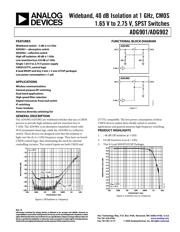
ADG901/ADG902
Rev. B | Page 5 of 16
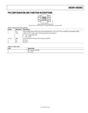
PIN CONFIGURATION AND FUNCTION DESCRIPTIONS
03336-004
ADG901/
ADG902
TOP VIEW
(Not to Scale)
V
DD
1
CTRL
2
GND
3
RF1
4
RF2
8
GND
7
GND
6
GND
5
Figure 4. 8-Lead MSOP (RM-8) and
8-Lead 3 mm × 3 mm LFCSP (CP-8 – Exposed pad tied to substrate, GND
Table 3. Pin Function Descriptions
Pin No. Mnemonic Description
1 V
DD
Power Supply Input. These parts can be operated from 1.65 V to 2.75 V; V
DD
should be decoupled to GND.
2 CTRL CMOS or LVTTL Logic Level. CTRL input should not exceed V
DD.
0 → RF1 Isolated from RF2.
1 → RF1 to RF2.
3, 5, 6, 7 GND Ground Reference Point for All Circuitry on the Part.
4 RF1 RF1 Port.
8 RF2 RF2 Port.
Table 4. Truth Table
CTRL Signal Path
0 RF1 isolated from RF2
1 RF1 to RF2
器件 Datasheet 文档搜索
AiEMA 数据库涵盖高达 72,405,303 个元件的数据手册,每天更新 5,000 多个 PDF 文件
