Datasheet 搜索 > 开发套件 > Silicon Labs(芯科) > C8051F020DK 数据手册 > C8051F020DK 数据手册 1/272 页

¥ 584.772
C8051F020DK 数据手册 - Silicon Labs(芯科)
制造商:
Silicon Labs(芯科)
分类:
开发套件
描述:
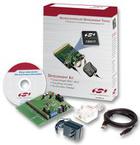
SILICON LABS C8051F020DK 开发套件, 100TQFP, 8051, 内置调试能力, 设置硬件断点
Pictures:
3D模型
符号图
焊盘图
引脚图
产品图
页面导航:
引脚图在P33P34P35P36P37P163P166P168Hot
原理图在P18P19P20P21P27P28P43P59P75P83P91P93
封装尺寸在P39P41
技术参数、封装参数在P31P58P74P82
应用领域在P130P225
电气规格在P32P58P74P82P89P92P94P99P133P136P140P161
导航目录
C8051F020DK数据手册
Page:
of 272 Go
若手册格式错乱,请下载阅览PDF原文件
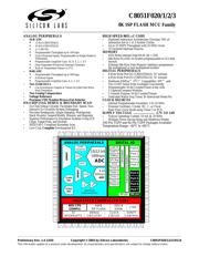
8K ISP FLASH MCU Family
C8051F020/1/2/3
Preliminary Rev. 1.4 12/03 Copyright © 2003 by Silicon Laboratories C8051F020/1/2/3-DS14
This information applies to a product under development. Its characteristics and specifications are subject to change without notice.
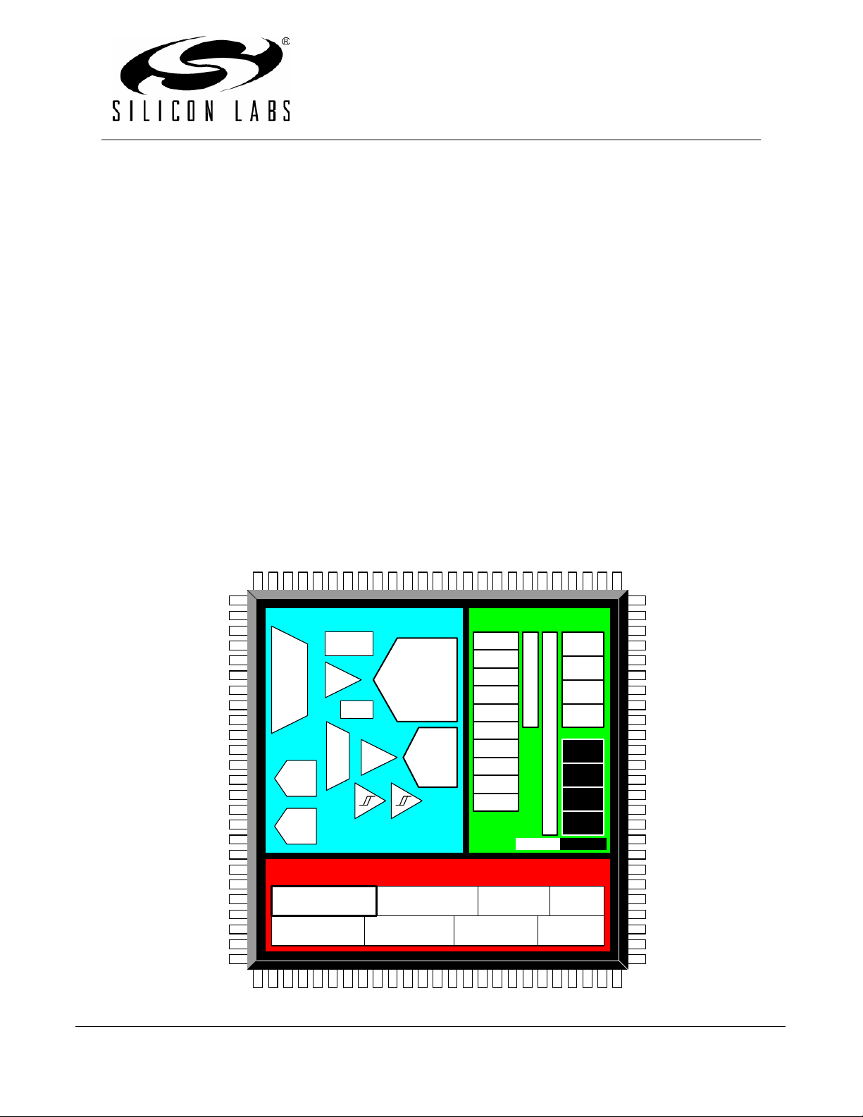
ANALOG PERIPHERALS
- SAR ADC
• 12-Bit (C8051F020/1)
• 10-Bit (C8051F022/3)
• ± 1 LSB INL
• Programmable Throughput up to 100 ksps
• Up to 8 External Inputs; Programmable as Single-Ended or
Differential
• Programmable Amplifier Gain: 16, 8, 4, 2, 1, 0.5
• Data-Dependent Windowed Interrupt Generator
• Built-in Temperature Sensor (± 3°C)
- 8-bit ADC
• Programmable Throughput up to 500 ksps
• 8 External Inputs
• Programmable Amplifier Gain: 4, 2, 1, 0.5
- Two 12-bit DACs
• Can Synchronize Outputs to Timers for Jitter-Free Wave-
form Generation
- Two Analog Comparators
- Voltage Reference
- Precision VDD Monitor/Brown-Out Detector
ON-CHIP JTAG DEBUG & BOUNDARY SCAN
-
On-Chip Debug Circuitry Facilitates Full- Speed, Non-
Intrusive In-Circuit/In-System Debugging
- Provides Breakpoints, Single-Stepping, Watchpoints,
Stack Monitor; Inspect/Modify Memory and Registers
- Superior Performance to Emulation Systems Using ICE-
Chips, Target Pods, and Sockets
- IEEE1149.1 Compliant Boundary Scan
- Low-Cost, Complete Development Kit
HIGH SPEED 8051 C CORE
-
Pipelined Instruction Architecture; Executes 70% of
Instruction Set in 1 or 2 System Clocks
- Up to 25 MIPS Throughput with 25 MHz Clock
- 22 Vectored Interrupt Sources
MEMORY
- 4352 Bytes Internal Data RAM (4k + 256)
- 64k Bytes FLASH; In-System programmable in 512-byte
Sectors
- External 64k Byte Data Memory Interface (programma-
ble multiplexed or non-
multiplexed modes)
DIGITAL PERIPHERALS
-
8 Byte-Wide Port I/O (C8051F020/2); 5V tolerant
- 4 Byte-Wide Port I/O (C8051F021/3); 5V tolerant
- Hardware SMBus™ (I
2
C™ Compatible), SPI™, and
Two UART Serial Ports Available Concurrently
- Programmable 16-bit Counter/Timer Array with
5 Capture/Compare Modules
- 5 General Purpose 16-bit Counter/Timers
- Dedicated Watch-Dog Timer; Bi-directional Reset Pin
CLOCK SOURCES
-
Internal Programmable Oscillator: 2-to-16 MHz
- External Oscillator: Crystal, RC, C, or Clock
- Real-Time Clock Mode using Timer 3 or PCA
SUPPLY VOLTAGE .......................... 2.7V TO 3.6V
- Typical Operating Current: 10 mA @ 20 MHz
- Multiple Power Saving Sleep and Shutdown Modes
100-Pin TQFP and 64-Pin TQFP Packages Available
Temperature Range: -40°C to +85°C
JTAG
64KB
ISP FLASH
4352 B
SRAM
SANITY
CONTROL
+
-
10/12-bit
100ksps
ADC
CLOCK
CIRCUIT
PGA
VREF
12-Bit
DAC
TEMP
SENSOR
VOLTAGE
COMPARATORS
ANALOG PERIPHERALS
Port 0
Port 1
Port 2
Port 3
CROSSBAR
DIGITAL I/O
HIGH-SPEED CONTROLLER CORE
DEBUG
CIRCUITRY
22
INTERRUPTS
8051 CPU
(25MIPS)
12-Bit
DAC
+
-
8-bit
500ksps
ADC
Port 4
Port 5
Port 6
Port 7
External Memory Interface
100 pin
64 pin
PGA
UART0
SMBus
SPI Bus
PCA
Timer 0
Timer 1
Timer 2
Timer 3
Timer 4
UART1
AMUX
AMUX
器件 Datasheet 文档搜索
AiEMA 数据库涵盖高达 72,405,303 个元件的数据手册,每天更新 5,000 多个 PDF 文件
