Datasheet 搜索 > 开发套件 > Silicon Labs(芯科) > C8051F020DK 数据手册 > C8051F020DK 数据手册 3/272 页

¥ 581.709
C8051F020DK 数据手册 - Silicon Labs(芯科)
制造商:
Silicon Labs(芯科)
分类:
开发套件
描述:
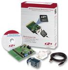
SILICON LABS C8051F020DK 开发套件, 100TQFP, 8051, 内置调试能力, 设置硬件断点
Pictures:
3D模型
符号图
焊盘图
引脚图
产品图
页面导航:
引脚图在P33P34P35P36P37P163P166P168Hot
原理图在P18P19P20P21P27P28P43P59P75P83P91P93
封装尺寸在P39P41
技术参数、封装参数在P31P58P74P82
应用领域在P130P225
电气规格在P32P58P74P82P89P92P94P99P133P136P140P161
导航目录
C8051F020DK数据手册
Page:
of 272 Go
若手册格式错乱,请下载阅览PDF原文件

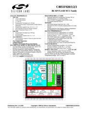
C8051F020/1/2/3
Rev. 1.4 3
TABLE OF CONTENTS
1. SYSTEM OVERVIEW .........................................................................................................17
1.1. CIP-51™ Microcontroller Core ......................................................................................22
1.1.1. Fully 8051 Compatible ..........................................................................................22
1.1.2. Improved Throughput............................................................................................22
1.1.3. Additional Features................................................................................................23
1.2. On-Chip Memory ............................................................................................................24
1.3. JTAG Debug and Boundary Scan ...................................................................................25
1.4. Programmable Digital I/O and Crossbar.........................................................................26
1.5. Programmable Counter Array .........................................................................................27
1.6. Serial Ports.......................................................................................................................27
1.7. 12-Bit Analog to Digital Converter.................................................................................28
1.8. 8-Bit Analog to Digital Converter...................................................................................29
1.9. Comparators and DACs...................................................................................................30
2. ABSOLUTE MAXIMUM RATINGS..................................................................................31
3. GLOBAL DC ELECTRICAL CHARACTERISTICS......................................................32
4. PINOUT AND PACKAGE DEFINITIONS........................................................................33
5. ADC0 (12-BIT ADC, C8051F020/1 ONLY) ........................................................................43
5.1. Analog Multiplexer and PGA..........................................................................................43
5.2. ADC Modes of Operation ...............................................................................................44
5.2.1. Starting a Conversion.............................................................................................44
5.2.2. Tracking Modes.....................................................................................................45
5.2.3. Settling Time Requirements ..................................................................................46
5.3. ADC0 Programmable Window Detector.........................................................................53
6. ADC0 (10-BIT ADC, C8051F022/3 ONLY) ........................................................................59
6.1. Analog Multiplexer and PGA..........................................................................................59
6.2. ADC Modes of Operation ...............................................................................................60
6.2.1. Starting a Conversion.............................................................................................60
6.2.2. Tracking Modes.....................................................................................................61
6.2.3. Settling Time Requirements ..................................................................................62
6.3. ADC0 Programmable Window Detector.........................................................................69
7. ADC1 (8-BIT ADC) ...............................................................................................................75
7.1. Analog Multiplexer and PGA..........................................................................................75
7.2. ADC1 Modes of Operation .............................................................................................76
7.2.1. Starting a Conversion.............................................................................................76
7.2.2. Tracking Modes.....................................................................................................76
7.2.3. Settling Time Requirements ..................................................................................78
8. DACS, 12-BIT VOLTAGE MODE......................................................................................83
8.1. DAC Output Scheduling..................................................................................................83
8.1.1. Update Output On-Demand...................................................................................84
8.1.2. Update Output Based on Timer Overflow.............................................................84
8.2. DAC Output Scaling/Justification...................................................................................84
9. VOLTAGE REFERENCE (C8051F020/2)..........................................................................91
器件 Datasheet 文档搜索
AiEMA 数据库涵盖高达 72,405,303 个元件的数据手册,每天更新 5,000 多个 PDF 文件
