Datasheet 搜索 > 稳压芯片 > Richtek(立锜) > RT9011-KSGQWC 数据手册 > RT9011-KSGQWC 数据手册 5/15 页

¥ 1.51
RT9011-KSGQWC 数据手册 - Richtek(立锜)
制造商:
Richtek(立锜)
分类:
稳压芯片
封装:
WFDFN-6
Pictures:
3D模型
符号图
焊盘图
引脚图
产品图
页面导航:

导航目录
RT9011-KSGQWC数据手册
Page:
of 15 Go
若手册格式错乱,请下载阅览PDF原文件
RT9011
5
DS9011-08 April 2011 www.richtek.com
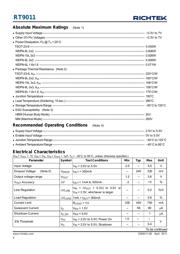
Note 1. Stresses listed as the above "Absolute Maximum Ratings" may cause permanent damage to the device. These are for
stress ratings. Functional operation of the device at these or any other conditions beyond those indicated in the
operational sections of the specifications is not implied. Exposure to absolute maximum rating conditions for extended
periods may remain possibility to affect device reliability.
Note 2. θ
JA
is measured in the natural convection at T
A
= 25°C on a low effective single layer thermal conductivity test board of
JEDEC 51-3 thermal measurement standard.
Note 3. Devices are ESD sensitive. Handling precaution recommended.
Note 4. The device is not guaranteed to function outside its operating conditions.
Note 5. The dropout voltage is defined as V
IN
-V
OUT
, which is measured when V
OUT
is V
OUT(NORMAL)
− 100mV.
Note 6. It is guaranteed by design.
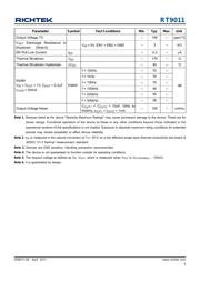
Parameter Symbol Test Conditions Min Typ Max Unit
Output Voltage TC -- 100 -- ppm/°C
V
OU T
Discharge Resistance in
Shutdown (Note 6)
V
IN
= 5V, EN1 = EN2 = GND
-- 3 -- kΩ
EN Pull Low Current
I
EN
-- 0.2 -- μA
Thermal Shutdown
T
SD
-- 170 --
°C
Thermal Shutdown Hysteresis
ΔT
SD
-- 40 -- °C
f = 100Hz
-- 70 --
f = 1kHz -- 70 --
f = 10kHz -- 70 --
f = 100kHz -- 54 --
f = 200kHz
-- 45 --
PSRR
V
IN
= V
OUT
+ 1V, C
OUT
= 2.2μF
I
LOAD
= 50mA
PSRR
f = 300kHz
-- 38 --
dB
Output Voltage Noise
C
OU T1
= C
OUT2
= 10uF, 10Hz to
100kHz, I
OUT1
= I
OUT2
= 1mA
-- 100 -- uVrms
器件 Datasheet 文档搜索
AiEMA 数据库涵盖高达 72,405,303 个元件的数据手册,每天更新 5,000 多个 PDF 文件
