Datasheet 搜索 > DSP数字信号处理器 > TI(德州仪器) > TMS320C40GFL50 数据手册 > TMS320C40GFL50 数据手册 4/44 页


¥ 5997.014
TMS320C40GFL50 数据手册 - TI(德州仪器)
制造商:
TI(德州仪器)
分类:
DSP数字信号处理器
封装:
CPGA-325
描述:
数字信号处理器 DIGITAL SIGNAL PROCESSOR
Pictures:
3D模型
符号图
焊盘图
引脚图
产品图
页面导航:
导航目录
TMS320C40GFL50数据手册
Page:
of 44 Go
若手册格式错乱,请下载阅览PDF原文件
TMS320C40
DIGITAL SIGNAL PROCESSOR
SPRS038 – JANUARY 1996
4
POST OFFICE BOX 1443 • HOUSTON, TEXAS 77251–1443
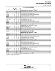
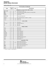
functions
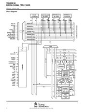
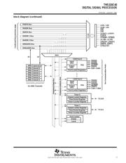
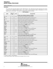
This section lists signal descriptions for the ’320C40 device. The ’320C40 pin functions table lists each signal,
number of pins, operating mode(s) (that is, input, output, or high-impedance state as indicated by I, O, or Z,
respectively), and function. The signals are grouped according to function.
Pin Functions
NAME
NO. OF
PINS
TYPE
†
DESCRIPTION
GLOBAL-BUS EXTERNAL INTERFACE (80 PINS)
D31–D0 32 I/O/Z 32-bit data port of the global-bus external interface
DE 1 I Data-bus-enable signal for the global-bus external interface
A30–A0 31 O/Z 31-bit address port of the global-bus external interface
AE 1 I Address-bus-enable signal for the global-bus external interface
STAT3–STAT0 4 O Status signals for the global-bus external interface
LOCK 1 O Lock signal for the global-bus external interface
STRB0
‡
1 O/Z Access strobe 0 for the global-bus external interface
R/W0
‡
1 O/Z Read/write signal for STRB0 accesses
PAGE0
‡
1 O/Z Page signal for STRB0 accesses
RDY0
‡
1 I Ready signal for STRB0 accesses
CE0
‡
1 I Control enable for the STRB0, PAGE0, and R/W0 signals
STRB1
‡
1 O/Z Access strobe 1 for the global-bus external interface
R/W1
‡
1 O/Z Read/write signal for STRB1 accesses
PAGE1
‡
1 O/Z Page signal for STRB1 accesses
RDY1
‡
1 I Ready signal for STRB1 accesses
CE1
‡
1 I Control enable for the STRB1, PAGE1, and R/W1 signals
LOCAL-BUS EXTERNAL INTERFACE (80 PINS)
LD31–LD0 32 I/O/Z 32-bit data port of the local-bus external interface
LDE 1 I Data-bus-enable signal for the local-bus external interface
LA30–LA0 31 O/Z 31-bit address port of the local-bus external interface
LAE 1 I Address-bus-enable signal for the local-bus external interface
LSTAT3–LSTAT0 4 O Status signals for the local-bus external interface
LLOCK 1 O Lock signal for the local-bus external interface
LSTRB0
‡
1 O/Z Access strobe 0 for the local-bus external interface
LR/W0 1 O/Z Read/write signal for LSTRB0 accesses
LPAGE0 1 O/Z Page signal for LSTRB0 accesses
LRDY0 1 I Ready signal for LSTRB0 accesses
LCE0 1 I Control enable for the LSTRB0, LPAGE0, and LR/W0 signals
LSTRB1
‡
1 O/Z Access strobe 1 for the local-bus external interface
LR/W1 1 O/Z Read/write signal for LSTRB1 accesses
LPAGE1 1 O/Z Page signal for LSTRB1 accesses
LRDY1 1 I Ready signal for LSTRB1 accesses
LCE1 1 I Control enable for the LSTRB1, LPAGE1, and LR/W1 signals
†
I = input, O = output, Z = high impedance
‡
Signal’s effective address range is defined by the local/global STRB ACTIVE bits.
器件 Datasheet 文档搜索
AiEMA 数据库涵盖高达 72,405,303 个元件的数据手册,每天更新 5,000 多个 PDF 文件
