Datasheet 搜索 > FET驱动器 > TI(德州仪器) > UCC37322P 数据手册 > UCC37322P 数据手册 5/31 页

 器件3D模型
¥ 9.65
UCC37322P 数据手册 - TI(德州仪器)
制造商:
TI(德州仪器)
分类:
FET驱动器
封装:
DIP-8
描述:
TEXAS INSTRUMENTS UCC37322P 芯片, MOSFET, 低压侧, 4V-15V电源, 9A输出, 35ns延迟, DIP-8
Pictures:
3D模型
符号图
焊盘图
引脚图
产品图
页面导航:
引脚图在P5Hot
封装尺寸在P19P20P21P23P24
型号编码规则在P2
标记信息在P19P20P21
封装信息在P5P19P20P21P22P23P24
技术参数、封装参数在P2
应用领域在P1P22P31
电气规格在P3
导航目录
UCC37322P数据手册
Page:
of 31 Go
若手册格式错乱,请下载阅览PDF原文件
1
2
3
4
8
7
6
5
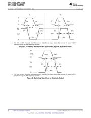
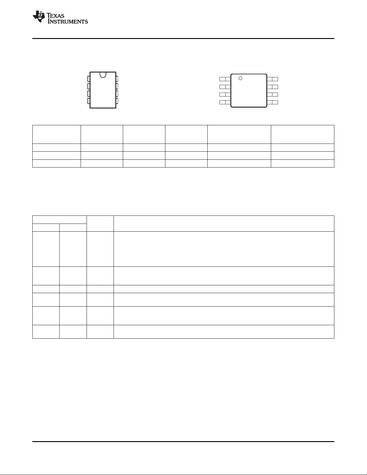
VDD
IN
ENBL
AGND
VDD
OUT
OUT
PGND
PDIP (P) PACKAGE
(TOP VIEW)
SOIC (D) OR MSOP (DGN) PACKAGE
(TOP VIEW)
VDD
OUT
OUT
PGND
8
7
6
5
1
2
3
4
VDD
IN
ENBL
AGND
UCC27321 , UCC27322
UCC37321, UCC37322
www.ti.com
SLUS504G –SEPTEMBER 2002–REVISED MAY 2013
PIN CONFIGURATIONS
POWER DISSIPATION RATING TABLE
Power Rating Derating Factor
PACKAGE SUFFIX θjc (°C/W) θja (°C/W) (mW) Above
T
A
= 70°C
(1)
70°C (mW/°C)
(1)
SOIC-8 D 42 84 – 160
(2)
344 – 655
(2)
6.25 – 11.9
(2)
PDIP-8 P 49 110 500 9
MSOP PowerPAD-8 DGN 4.7 50 – 59 1370 17.1
(1) 125°C operating junction temperature is used for power rating calculations
(2) The range of values indicates the effect of pc-board. These values are intended to give the system designer an indication of the best
and worst case conditions. In general, the system designer should attempt to use larger traces on the pc-board where possible in order
to spread the heat away form the device more effectively. For additional information on device temperature management, please refer to
Packaging Information section of the Power Supply Control Products Data Book, (Ti Literature Number SLUD003).
TERMINAL FUNCTIONS
TERMINAL
I/O DESCRIPTION
NAME NO.
The AGND and the PGND should be connected by a single thick trace directly under the device.
There should be a low ESR, low ESL capacitor of 0.1 µF between VDD (pin 8) and PGND and a
seperate 0.1-µF capacitor between VDD (pin 1) and AGND. The power MOSFETs should be located
AGND 4 –
on the PGND side of the device while the control circuit should be on the AGND side of the device.
The control circuit ground should be common with the AGND while the PGND should be common
with the source of the power FETs.
Enable input for the driver with logic compatible threshold and hysteresis. The driver output can be
ENBL 3 I enabled and disabled with this pin. It is internally pulled up to V
DD
with 100-kΩ resistor for active high
operation. The output state when the device is disabled will be low regardless of the input state.
IN 2 I Input signal of the driver which has logic compatible threshold and hysteresis.
Driver outputs that must be connected together externally. The output stage is capable of providing
OUT 6, 7 O
9-A peak drive current to the gate of a power MOSFET.
Common ground for output stage. This ground should be connected very closely to the source of the
PGND 5 – power MOSFET which the driver is driving. Grounds are separated to minimize ringing affects due to
output switching di/dt which can affect the input threshold.
Supply voltage and the power input connections for this device. Three pins must be connected
VDD 1, 8 I
together externally.
Copyright © 2002–2013, Texas Instruments Incorporated Submit Documentation Feedback 5
Product Folder Links: UCC27321 UCC27322 UCC37321 UCC37322
器件 Datasheet 文档搜索
AiEMA 数据库涵盖高达 72,405,303 个元件的数据手册,每天更新 5,000 多个 PDF 文件
