Datasheet 搜索 > 数字电位器 > ADI(亚德诺) > AD7376ARWZ50 数据手册 > AD7376ARWZ50 其他数据使用手册 4/20 页
 器件3D模型
¥ 45.411
AD7376ARWZ50 其他数据使用手册 - ADI(亚德诺)
制造商:
ADI(亚德诺)
分类:
数字电位器
封装:
SOIC-16
描述:
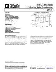
ANALOG DEVICES AD7376ARWZ50 易失性数字电位器, 50 kohm, 单, SPI, ± 30%, 4.5 V
Pictures:
3D模型
符号图
焊盘图
引脚图
产品图
页面导航:
导航目录
AD7376ARWZ50数据手册
Page:
of 20 Go
若手册格式错乱,请下载阅览PDF原文件
AD7376
Rev. C | Page 4 of 20
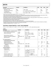
Parameter Symbol Conditions Min Typ
1
Max Unit
DYNAMIC CHARACTERISTICS
6, 9,10
Bandwidth −3 dB BW Code = 0x40 470 kHz
Total Harmonic Distortion THD
W
V
A
= 1 V rms, V
B
= 0 V, f = 1 kHz 0.006 %
V
W
Settling Time t
S
V
A
= 10 V, V
B
= 0 V, ±1 LSB error band 4 μs
Resistor Noise Voltage e
N_WB
R
WB
= 5 kΩ, f = 1 kHz 0.9 nV√Hz
1
Typical values represent average readings at 25°C, V
DD
= 15 V, and V
SS
= −15 V.
2
Resistor position nonlinearity error R-INL is the deviation from an ideal value measured between the maximum and minimum resistance wiper positions. R-DNL
measures the relative step change from an ideal value measured between successive tap positions. Parts are guaranteed monotonic.
3
Pb-free parts have a 35 ppm/°C temperature coefficient (tempco).
4
INL and DNL are measured at V
W
with the RDAC configured as a potentiometer divider, similar to a voltage output digital-to-analog converter. V
A
= V
DD
and V
B
= 0 V.
DNL specification limits of ±1 LSB maximum are guaranteed monotonic operating conditions.
5
Resistor Terminals A, B, and W have no limitations on polarity with respect to each other.
6
Guaranteed by design and not subject to production test.
7
Measured at the A terminal. A terminal is open circuit in shutdown mode.
8
P
DISS
is calculated from (I
DD
× V
DD
) + abs(I
SS
× V
SS
). CMOS logic level inputs result in minimum power dissipation.
9
Bandwidth, noise, and settling times are dependent on the terminal resistance value chosen. The lowest R value results in the fastest settling time and highest
bandwidth. The highest R value results in the minimum overall power consumption.
10
All dynamic characteristics use V
DD
= 15 V and V
SS
= −15 V.
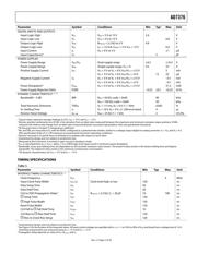
ELECTRICAL CHARACTERISTICS—50 kΩ, 100 kΩ VERSIONS
V
DD
/V
SS
= ±15 V ± 10% or ±5 V ± 10%, V
A
= V
DD
, V
B
= V
SS
/0 V, −40°C < T
A
< +85°C, unless otherwise noted.
Table 2.
Parameter Symbol Conditions Min Typ
1
Max Unit
DC CHARACTERISTICS—RHEOSTAT MODE
Resistor Differential Nonlinearity
2
R-DNL R
WB
, V
A
= NC −1 ±0.5 +1 LSB
Resistor Nonlinearity
2
R-INL R
WB
, V
A
= NC, R
AB
= 50 kΩ −1.5 ±0.5 +1.5 LSB
R
WB
, V
A
= NC, R
AB
= 100 kΩ −1 ±0.5 +1 LSB
Nominal Resistor Tolerance ∆R
AB
T
A
= 25°C −30 +30 %
Resistance Temperature Coefficient
3
(∆R
AB
/R
AB
)/∆T × 10
6
V
AB
= V
DD
, wiper = no connect −300 ppm/°C
Wiper Resistance R
W
V
DD
/V
SS
= ±15 V 120 200 Ω
V
DD
/V
SS
= ±5 V 260 Ω
DC CHARACTERISTICS—
POTENTIOMETER DIVIDER MODE
Integral Nonlinearity
4
INL −1 ±0.5 +1 LSB
Differential Nonlinearity
4
DNL −1 ±0.5 +1 LSB
Voltage Divider Temperature
Coefficient
(∆V
W
/V
W
)/∆T × 10
6
Code = 0x40 5 ppm/°C
Full-Scale Error V
WFSE
Code = 0x7F −2 −0.5 0 LSB
Zero-Scale Error V
WZSE
Code = 0x00 0 0.5 1 LSB
RESISTOR TERMINALS
Voltage Range
5
V
A, B, W
V
SS
V
DD
V
Capacitance
6
A, B C
A, B
f = 1 MHz, measured to GND,
code = 0x40
45 pF
Capacitance
6
C
W
f = 1 MHz, measured to GND,
code = 0x40
60 pF
Shutdown Supply Current
7
I
A_SD
V
A
= V
DD
, V
B
= 0 V, SHDN = 0
0.02 1 μA
Shutdown Wiper Resistance R
W_SD
V
A
= V
DD
, V
B
= 0 V, SHDN = 0, V
DD
= 15 V
170 400 Ω
Common-Mode Leakage I
CM
V
A
= V
B
= V
W
1 nA
器件 Datasheet 文档搜索
AiEMA 数据库涵盖高达 72,405,303 个元件的数据手册,每天更新 5,000 多个 PDF 文件
