Datasheet 搜索 > ADI(亚德诺) > AD8045 数据手册 > AD8045 其他数据使用手册 3/8 页


¥ 0
AD8045 其他数据使用手册 - ADI(亚德诺)
制造商:
ADI(亚德诺)
描述:
3内华达州/ Hz的超低失真,高速运算放大器 3 nV/Hz Ultralow Distortion, High Speed Op Amp
Pictures:
3D模型
符号图
焊盘图
引脚图
产品图
页面导航:
应用领域在P8
导航目录
AD8045数据手册
Page:
of 8 Go
若手册格式错乱,请下载阅览PDF原文件
–3–
BIPOLAR
SIGNAL
+/–0.5 V
+5V
R1
499Ω
AD8037
1N5712
0.1µF
+5V
806Ω
100Ω
V
H
= +0.55V
49.9Ω
V
L
= –0.55V
0.1µF
–5.2V
806Ω 100Ω
AD9002
FLASH CONVERTER
(8-BITS, 125 MSPS)
0.1µF
–5.2V
R2
301Ω
V
IN
= –1 +/–1V
SUBSTRATE
DIODE
R
T
75Ω
R3
750Ω
0.1µF
AD780
+2.5 V REF
10µF
+
AD8037 OUTPUT
CLAMPS AT +0.1 V, –2.1 V
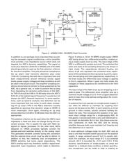
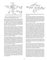
Figure 2. AD9002, 8-Bit, 125 MSPS Flash Converter
In addition to and perhaps more important than provid-
ing the necessary signal conditioning, a drive amplifier
must provide a low impedance source which does not
degrade the ADC’s dynamic capabilities. The signal to
noise plus distortion (S/(N+D) or SINAD) plot of the ADC
should generally be used as the first selection criterion
for the drive amplifier. This plot should be compared to
the op amp’s total harmonic distortion plus noise
(THD+N). Comparing like with like is important here and
both measurements should reference similar signal
levels, power supply voltages and bias conditions as will
be used in the actual circuit. The amplifier’s loading con-
ditions should also be similar to those presented by the
ADC. As a general rule, in order to prevent the op amp
from degrading the dynamic performance of the ADC,
its THD+N should be 6 dB to 10 dB better than the ADC’s
S/(N+D) at the highest signal frequency
3
(usually but not
always the ADC’s Nyquist frequency). In some applica-
tions, such as spectral analysis, low distortion can be
more important than low noise. In such cases, compar-
ing the op amp’s THD to the ADC’s distortion (usually
specified as spurious free dynamic range or SFDR) is
more meaningful. Once again, choosing an op amp
whose distortion is 6 dB to 10 dB better than the ADC’s is
appropriate.
This selection criterion can be used where the ADC’s input
impedance is fixed and does not change during the con-
version process. This is usually the case with ADCs de-
signed on bipolar processes. On the other hand, ADCs
designed on CMOS processes typically connect the
sample-and-hold switches directly to the analog input.
This generates transient currents during the conversion
that the external drive circuit must be able to deliver. In
addition to this, the (relatively low) on-impedance of
CMOS switches has some signal dependency. The
ADC’s analog input may, therefore, exhibit a signal-level-
dependent input impedance, which leads to distortion.
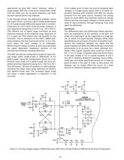
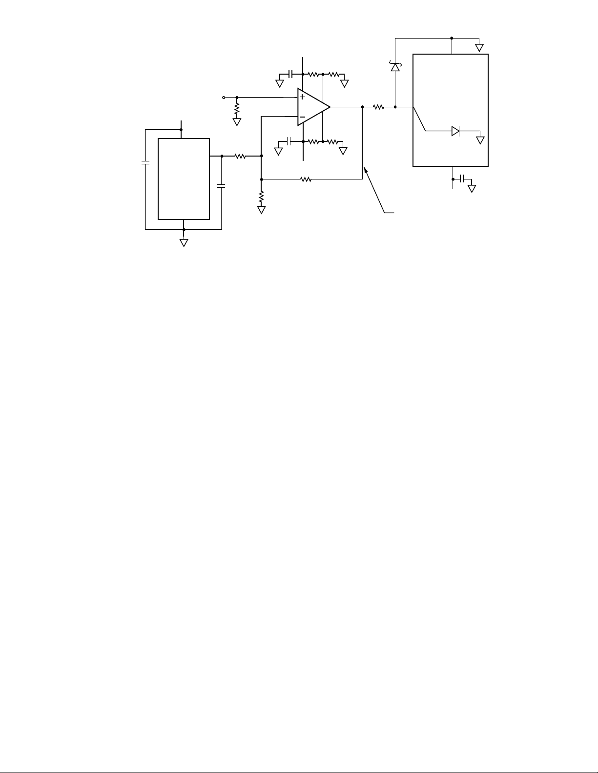
Figure 3 shows a 12-bit 10 MSPS single-supply CMOS
ADC being driven by a differential amplifier, created us-
ing a single-supply dual op amp. The input stage of the
ADC is a differential sample-and-hold. The switches that
open and close at the sampling frequency are shown in
track mode. The capacitances denoted C
PAR
C
PIN
are
about 16 pF and represent the combined stray capaci-
tance of the switches and the input pins. C
S
and C
H
repre-
sent the sampling and hold capacitances respectively. In
the track mode, the differential input voltage is applied
to the C
S
capacitors. When it goes into hold mode, the
voltages on these capacitors are transferred to the hold
capacitors.
The input range of the ADC is set, by pin strapping, to 2 V
peak-to-peak. The differential drive amplifier sets up a
common-mode voltage of 2.5 V. From a signal distortion
point of view, this is the optimal configuration for a num-
ber of reasons.
In systems that truly operate on a single power supply, it
can often be difficult to maintain dc coupling from
source all the way to the ADC. In such systems, a virtual
ground is often created, usually centered halfway be-
tween the rails. This introduces the question of an opti-
mum input voltage range for a single-supply ADC. At
first glance, it would seem that a zero-volt referenced in-
put might be desirable. But in fact, this places some se-
vere constraints on both the ADC and its driving
amplifier because both must maintain full linearity and
low distortion at or near 0 V.
A more optimum voltage range for both ADC and op
amp is one that includes neither ground nor the positive
supply. A range centered around V
S
/2 is usually opti-
mum. For example, an input range of 2 V p-p centered
around +2.5 V is bounded by +1.5 V and +3.5 V. If the
dynamic specifications of single-supply op amps are
stated for a midscale bias condition, a direct specifica-
tion comparison can be made to help in making an
器件 Datasheet 文档搜索
AiEMA 数据库涵盖高达 72,405,303 个元件的数据手册,每天更新 5,000 多个 PDF 文件
