Datasheet 搜索 > 放大器、缓冲器 > ADI(亚德诺) > ADA4505-2ACBZ-RL 数据手册 > ADA4505-2ACBZ-RL 其他数据使用手册 6/21 页


¥ 3.761
ADA4505-2ACBZ-RL 其他数据使用手册 - ADI(亚德诺)
制造商:
ADI(亚德诺)
分类:
放大器、缓冲器
封装:
WLCSP-8
描述:
10 μA ,轨至轨I / O,零输入交越失真放大器 10 μA, Rail-to-Rail I/O, Zero Input Crossover Distortion Amplifiers
Pictures:
3D模型
符号图
焊盘图
引脚图
产品图
页面导航:
导航目录
ADA4505-2ACBZ-RL数据手册
Page:
of 21 Go
若手册格式错乱,请下载阅览PDF原文件
ADA4857-1/ADA4857-2 Data Sheet
Rev. C | Page 6 of 20
ABSOLUTE MAXIMUM RATINGS
Table 3.
Parameter Rating
Supply Voltage 11 V
Power Dissipation
See Figure 4
Common-Mode Input Voltage −V
S
+ 0.7 V to +V
S
− 0.7 V
Differential Input Voltage ±V
S
Exposed Paddle Voltage −V
S
Storage Temperature Range −65°C to +125°C
Operating Temperature Range −40°C to +125°C
Lead Temperature (Soldering, 10 sec) 300°C
Junction Temperature 150°C
Stresses above those listed under Absolute Maximum Ratings
may cause permanent damage to the device. This is a stress
rating only; functional operation of the device at these or any
other conditions above those indicated in the operational
section of this specification is not implied. Exposure to absolute
maximum rating conditions for extended periods may affect
device reliability.
THERMAL RESISTANCE
θ
JA
is specified for the worst-case conditions, that is, θ
JA
is specified
for device soldered in circuit board for surface-mount packages.
Table 4.
Package Type θ
JA
θ
JC
Unit
8-Lead SOIC 115 15 °C/W
8-Lead LFCSP 94.5 34.8 °C/W
16-Lead LFCSP 68.2 19 °C/W
MAXIMUM POWER DISSIPATION
The maximum safe power dissipation for the ADA4857 is
limited by the associated rise in junction temperature (T
J
) on
the die. At approximately 150°C, which is the glass transition
temperature, the properties of the plastic change. Even temporarily
exceeding this temperature limit may change the stresses that
the package exerts on the die, permanently shifting the parametric
performance of the ADA4857. Exceeding a junction temperature of
175°C for an extended period can result in changes in silicon
devices, potentially causing degradation or loss of functionality.
The power dissipated in the package (P
D
) is the sum of the
quiescent power dissipation and the power dissipated in the
die due to the ADA4857 drive at the output. The quiescent
power is the voltage between the supply pins (V
S
) times the
quiescent current (I
S
).
P
D
= Quiescent Power + (Total Drive Power − Load Power)
( )
L
OUT
L
OUTS
SS
D
R
V
R
V
V
IVP
2
–
2
×+×=
RMS output voltages should be considered. If R
L
is referenced
to −V
S
, as in single-supply operation, the total drive power is
V
S
× I
OUT
. If the rms signal levels are indeterminate, consider the
worst case, when V
OUT
= V
S
/4 for R
L
to midsupply.
( )
( )
L
S
SS
D
R
V
IVP
2
4/
+×=
In single-supply operation with R
L
referenced to −V
S
, the worst
case is V
OUT
= V
S
/2.
Airflow increases heat dissipation, effectively reducing θ
JA
.
In addition, more metal directly in contact with the package
leads and exposed paddle from metal traces, through holes,
ground, and power planes reduces θ
JA
.
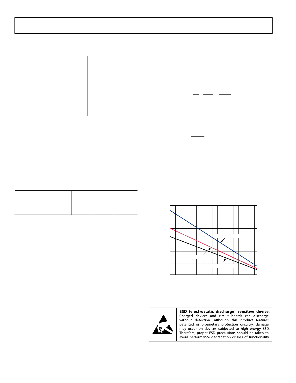
Figure 4 shows the maximum power dissipation in the package
vs. the ambient temperature for the SOIC and LFCSP packages
on a JEDEC standard 4-layer board. θ
JA
values are approximations.
0
0.5
1.0
1.5
2.0
2.5
3.0
–40–30–20 –10 0 10 20 30 40 50 60 70 80 90 100
110
120
07040-004
AMBIENT TEMPERATURE (°C)
MAXIMUM POWER DISSIPATION (W)
ADA4857-1 (SOIC)
ADA4857-1 (LFCSP)
ADA4857-2 (LFCSP)
Figure 4. Maximum Power Dissipation vs. Temperature for a 4-Layer Board
ESD CAUTION
器件 Datasheet 文档搜索
AiEMA 数据库涵盖高达 72,405,303 个元件的数据手册,每天更新 5,000 多个 PDF 文件
