Datasheet 搜索 > 接口芯片 > ADI(亚德诺) > ADN4666ARUZ 数据手册 > ADN4666ARUZ 其他数据使用手册 1/12 页
 器件3D模型
¥ 23.141
ADN4666ARUZ 其他数据使用手册 - ADI(亚德诺)
制造商:
ADI(亚德诺)
分类:
接口芯片
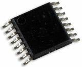
封装:
TSSOP-16
描述:
ANALOG DEVICES ADN4666ARUZ 驱动器, LVDS, 四路, 差分线路接收器, 15 mA, -40 °C, 85 °C, 3 V
Pictures:
3D模型
符号图
焊盘图
引脚图
产品图
页面导航:
导航目录
ADN4666ARUZ数据手册
Page:
of 12 Go
若手册格式错乱,请下载阅览PDF原文件
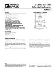
3 V, LVDS, Quad CMOS
Differential Line Receiver
ADN4666
Rev. 0
Information furnished by Analog Devices is believed to be accurate and reliable. However, no
responsibility is assumed by Analog Devices for its use, nor for any infringements of patents or other
rights of third parties that may result from its use. Specifications subject to change without notice. No
license is granted by implication or otherwise under any patent or patent rights of Analog Devices.
Trademarks and registered trademarks are the property of their respective owners.
One Technology Way, P.O. Box 9106, Norwood, MA 02062-9106, U.S.A.
Tel: 781.329.4700 www.analog.com
Fax: 781.461.3113 ©2009 Analog Devices, Inc. All rights reserved.
FEATURES
±8 kV ESD IEC 61000-4-2 contact discharge on receiver input pins
400 Mbps (200 MHz) switching rates
100 ps channel-to-channel skew (typical)
100 ps differential skew (typical)
3.3 ns propagation delay (maximum)
3.3 V power supply
High impedance outputs on power-down
Low power design (10 mW quiescent typical)
Interoperable with existing 5 V LVDS drivers
Accepts small swing (350 mV typical) differential
input signal levels
Supports open, short, and terminated input fail-safe
Conforms to TIA/EIA-644 LVDS standard
Industrial operating temperature range of −40°C to +85°C
Available in surface-mount SOIC package and low profile
TSSOP package
APPLICATIONS
Point-to-point data transmission
Multidrop buses
Clock distribution networks
Backplane receivers
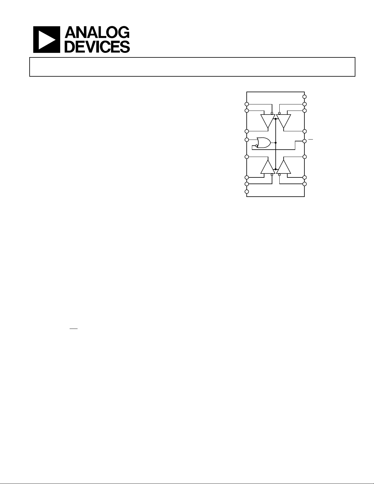
FUNCTIONAL BLOCK DIAGRAM
R
OUT1
R
OUT2
R
IN1+
R
IN1–
R
IN2+
R
IN2–
R
OUT4
R
OUT3
R
IN4–
R
IN3–
R
IN4+
R
IN3+
V
CC
GND
ADN4666
R1
R4
R2
R3
08097-001
EN
EN
Figure 1.
GENERAL DESCRIPTION
The ADN4666 is a quad-channel, CMOS low voltage differential
signaling (LVDS) line receiver offering data rates of over 400 Mbps
(200 MHz) and ultralow power consumption.
The device accepts low voltage (350 mV typical) differential
input signals and converts them to a single-ended, 3 V TTL/CMOS
logic level.
The ADN4666 also offers active high and active low enable/disable
inputs (EN and
EN
) that control all four receivers. These inputs
disable the receivers and switch the outputs to a high impedance
state. Consequently, the outputs of one or more ADN4666
devices can be multiplexed together to reduce the quiescent
power consumption to 10 mW typical.
The ADN4666 and its companion driver, the ADN4665, offer
a new solution to high speed, point-to-point data transmission
and offer a low power alternative to emitter-coupled logic (ECL)
or positive emitter-coupled logic (PECL).
器件 Datasheet 文档搜索
AiEMA 数据库涵盖高达 72,405,303 个元件的数据手册,每天更新 5,000 多个 PDF 文件
