Datasheet 搜索 > 接口芯片 > ADI(亚德诺) > ADN4666ARUZ 数据手册 > ADN4666ARUZ 其他数据使用手册 6/12 页
 器件3D模型
¥ 23.037
ADN4666ARUZ 其他数据使用手册 - ADI(亚德诺)
制造商:
ADI(亚德诺)
分类:
接口芯片
封装:
TSSOP-16
描述:
ANALOG DEVICES ADN4666ARUZ 驱动器, LVDS, 四路, 差分线路接收器, 15 mA, -40 °C, 85 °C, 3 V
Pictures:
3D模型
符号图
焊盘图
引脚图
产品图
页面导航:
导航目录
ADN4666ARUZ数据手册
Page:
of 12 Go
若手册格式错乱,请下载阅览PDF原文件
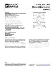
ADN4666
Rev. 0 | Page 6 of 12
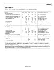
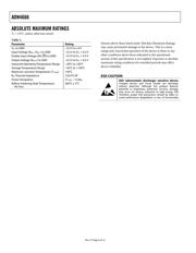
ABSOLUTE MAXIMUM RATINGS
T
A
= 25°C, unless otherwise noted.
Table 3.
Parameter Rating
V
CC
to GND −0.3 V to +4 V
Input Voltage (R
INx+
, R
INx−
) to GND −0.3 V to V
CC
+ 0.3 V
Enable Input Voltage (EN, EN) to GND
−0.3 V to V
CC
+ 0.3 V
Output Voltage (R
OUTx
) to GND −0.3 V to V
CC
+ 0.3 V
Industrial Operating Temperature Range −40°C to +85°C
Storage Temperature Range −65°C to +150°C
Maximum Junction Temperature (T
J MAX
) 150°C
θ
JA
Thermal Impedance 150.4°C/W
Power Dissipation (T
J MAX
− T
A
)/θ
JA
Reflow Soldering Peak Temperature,
Pb-Free
260°C ± 5°C
Stresses above those listed under Absolute Maximum Ratings
may cause permanent damage to the device. This is a stress
rating only; functional operation of the device at these or any
other conditions above those indicated in the operational
section of this specification is not implied. Exposure to absolute
maximum rating conditions for extended periods may affect
device reliability.
ESD CAUTION
器件 Datasheet 文档搜索
AiEMA 数据库涵盖高达 72,405,303 个元件的数据手册,每天更新 5,000 多个 PDF 文件
