Datasheet 搜索 > 存储芯片 > Microchip(微芯) > AT24C01C-STUM-T 数据手册 > AT24C01C-STUM-T 其他数据使用手册 5/45 页

¥ 1.056
AT24C01C-STUM-T 其他数据使用手册 - Microchip(微芯)
制造商:
Microchip(微芯)
分类:
存储芯片
封装:
SOT-23-5
描述:
电可擦除可编程只读存储器 1K 2-WIRE 5 SOT23 PB/HALO FREE, 1.7V
Pictures:
3D模型
符号图
焊盘图
引脚图
产品图
页面导航:
引脚图在P5P6Hot
原理图在P8
封装尺寸在P24P38P42
型号编码规则在P24
标记信息在P24
封装信息在P24P25P26P27P28P29P30P31P32P33P34P35
技术参数、封装参数在P9P11
电气规格在P9P10P11P12
型号编号列表在P42
导航目录
AT24C01C-STUM-T数据手册
Page:
of 45 Go
若手册格式错乱,请下载阅览PDF原文件
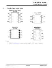
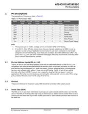
2. Pin Descriptions
The descriptions of the pins are listed in Table 2-1.
Table 2-1. Pin Function Table
Name 8-Lead
PDIP
8-Lead
SOIC
8-Lead
TSSOP
5-Lead
SOT23
8-Pad
UDFN
(1)
8-Ball
VFBGA
Function
A0
(2)
1 1 1 - 1 1 Device Address Input
A1
(2)
2 2 2 - 2 2 Device Address Input
A2
(2)
3 3 3 - 3 3 Device Address Input
GND 4 4 4 2 4 4 Ground
SDA 5 5 5 3 5 5 Serial Data
SCL 6 6 6 1 6 6 Serial Clock
WP
(2)
7 7 7 5 7 7 Write-Protect
V
CC
8 8 8 4 8 8 Device Power Supply
Note:
1. The exposed pad on the this package can be connected to GND or left floating.
2. If the A0, A1, A2 or WP pins are not driven, they are internally pulled down to GND. In order to
operate in a wide variety of application environments, the pull-down mechanism is intentionally
designed to be somewhat strong. Once these pins are biased above the CMOS input buffer’s trip
point (~0.5 x V
CC
), the pull‑down mechanism disengages. Microchip recommends connecting these
pins to a known state whenever possible.
2.1 Device Address Inputs (A0, A1, A2)
The A0, A1 and A2 pins are device address inputs that are hard-wired (directly to GND or to V
CC
) for
compatibility with other two-wire Serial EEPROM devices. When the pins are hard-wired, as many as
eight devices may be addressed on a single bus system. A device is selected when a corresponding
hardware and software match is true. If these pins are left floating, the A0, A1 and A2 pins will be
internally pulled down to GND. However, due to capacitive coupling that may appear in customer
applications, Microchip recommends always connecting the address pins to a known state. When using a
pull‑up resistor, Microchip recommends using 10 kΩ or less.
2.2 Ground
The ground reference for the power supply. GND should be connected to the system ground.
2.3 Serial Data (SDA)
The SDA pin is an open-drain bidirectional input/output pin used to serially transfer data to and from the
device. The SDA pin must be pulled high using an external pull-up resistor (not to exceed 10 kΩ in value)
and may be wire-ORed with any number of other open-drain or open-collector pins from other devices on
the same bus.
AT24C01C/AT24C02C
Pin Descriptions
© 2018 Microchip Technology Inc.
Datasheet
DS20006111A-page 5
器件 Datasheet 文档搜索
AiEMA 数据库涵盖高达 72,405,303 个元件的数据手册,每天更新 5,000 多个 PDF 文件
