Datasheet 搜索 > DA转换器 > Cirrus Logic(思睿逻辑) > CS4353-CNZ 数据手册 > CS4353-CNZ 产品手册 2/24 页
 器件3D模型
¥ 5.301
CS4353-CNZ 产品手册 - Cirrus Logic(思睿逻辑)
制造商:
Cirrus Logic(思睿逻辑)
分类:
DA转换器
封装:
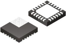
QFN-24
描述:
24 位,Cirrus Logic### 数模转换器 - Cirrus Logic
Pictures:
3D模型
符号图
焊盘图
引脚图
产品图
页面导航:
导航目录
CS4353-CNZ数据手册
Page:
of 24 Go
若手册格式错乱,请下载阅览PDF原文件

2 DS786A1
CS4412A
TABLE OF CONTENTS
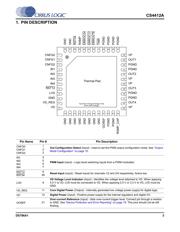
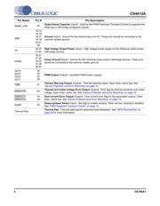
1. PIN DESCRIPTION ................................................................................................................................. 3
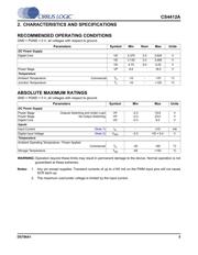
2. CHARACTERISTICS AND SPECIFICATIONS ...................................................................................... 5
RECOMMENDED OPERATING CONDITIONS .................................................................................... 5
ABSOLUTE MAXIMUM RATINGS ........................................................................................................ 5
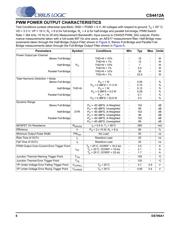
PWM POWER OUTPUT CHARACTERISTICS ..................................................................................... 6
DC ELECTRICAL CHARACTERISTICS ................................................................................................ 7
DIGITAL INTERFACE SPECIFICATIONS ............................................................................................. 7
DIGITAL I/O PIN CHARACTERISTICS ................................................................................................. 8
3. TYPICAL CONNECTION DIAGRAMS ................................................................................................. 9
4. APPLICATIONS ................................................................................................................................... 13
4.1 Overview ........................................................................................................................................ 13
4.2 Reset and Power-Up ...................................................................................................................... 13
4.2.1 PWM Popguard Transient Control ........................................................................................ 13
4.2.2 Initial Pulse Edge Delay ........................................................................................................ 14
4.2.3 Recommended Power-Up Sequence .................................................................................... 14
4.2.4 Recommended Power-Down Sequence ............................................................................... 14
4.3 Output Mode Configuration ............................................................................................................ 15
4.4 Output Filters ................................................................................................................................. 16
4.4.1 Half-Bridge Output Filter ........................................................................................................ 16
4.4.2 Full-Bridge Output Filter (Stereo or Parallel) ......................................................................... 18
4.5 Device Protection and Error Reporting .......................................................................................... 19
4.5.1 Over-Current Protection ........................................................................................................ 19
4.5.2 Thermal Warning, Thermal Error, and Under-Voltage Error ................................................. 19
5. POWER SUPPLY, GROUNDING, AND PCB LAYOUT ....................................................................... 20
5.1 Power Supply and Grounding ........................................................................................................ 20
5.1.1 Integrated VD Regulator ........................................................................................................ 20
5.2 QFN Thermal Pad .......................................................................................................................... 20
6. PARAMETER DEFINITIONS ................................................................................................................ 21
7. PACKAGE DIMENSIONS .................................................................................................................... 22
8. THERMAL CHARACTERISTICS ......................................................................................................... 23
8.1 Thermal Flag .................................................................................................................................. 23
9. ORDERING INFORMATION ................................................................................................................ 24
10. REVISION HISTORY .......................................................................................................................... 24
LIST OF FIGURES
Figure 1.Stereo Full-Bridge Typical Connection Diagram ........................................................................... 9
Figure 2.2.1 Channel Typical Connection Diagram .................................................................................. 10
Figure 3.4 Channel Half-Bridge Typical Connection Diagram .................................................................. 11
Figure 4.Parallel Full-Bridge Typical Connection Diagram .......................................................................12
Figure 5.Output Filter - Half-Bridge ........................................................................................................... 16
Figure 6.Output Filter - Full-Bridge ............................................................................................................ 18
LIST OF TABLES
Table 1. I/O Power Rails ............................................................................................................................. 8
Table 2. Typical Ramp Times for Typical VP Voltages ............................................................................. 13
Table 3. Output Mode Configuration Options ............................................................................................ 15
Table 4. Low-Pass Filter Components - Half-Bridge ................................................................................. 16
Table 5. DC-Blocking Capacitors Values - Half-Bridge ............................................................................. 17
Table 6. Low-Pass Filter Components - Full-Bridge ................................................................................. 18
Table 7. Over-current Error Conditions ..................................................................................................... 19
Table 8. Thermal and Under-Voltage Error Conditions ............................................................................. 19
Table 9. Power Supply Configuration and Settings ................................................................................... 20
器件 Datasheet 文档搜索
AiEMA 数据库涵盖高达 72,405,303 个元件的数据手册,每天更新 5,000 多个 PDF 文件
