Datasheet 搜索 > 数模转换器 > Cirrus Logic(思睿逻辑) > CS5343-DZZR 数据手册 > CS5343-DZZR 其他数据使用手册 4/24 页
 器件3D模型
¥ 13.862
CS5343-DZZR 其他数据使用手册 - Cirrus Logic(思睿逻辑)
制造商:
Cirrus Logic(思睿逻辑)
分类:
数模转换器
封装:
TSSOP-10
Pictures:
3D模型
符号图
焊盘图
引脚图
产品图
页面导航:
典型应用电路图在P7
原理图在P14
导航目录
CS5343-DZZR数据手册
Page:
of 24 Go
若手册格式错乱,请下载阅览PDF原文件
4 DS687DB2
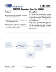
CDB5343
1. SYSTEM OVERVIEW
The CDB5343 evaluation board is an excellent tool for evaluating the CS5343 Analog-to-Digital Converter (ADC).
A minimum number of passive components condition the analog input signal prior to the CS5343, and the on-board
CS8406 digital audio interface transmitter provides an easy interface to digital audio signal analyzers including the
majority of digital audio test equipment. Additionally, the CDB5343 features an interface header (J3) for clock and
data I/O.
Figures 19 through Figures 27 show the CDB5343 schematic and layout.
1.1 CS5343
The CS5343 ADC performs stereo 24-bit A/D conversion at sample rates of up to 108 kHz and generates
I²S audio format data. Furthermore, in both Master and Slave Modes the CS5343 supports MCLK/LRCK
ratios of 256x and 384x. The CS5343 product datasheet contains complete device information.
2. CS8406 DIGITAL AUDIO TRANSMITTER
The CS8406 converts the CS5343 output to a standard S/PDIF data stream. Given an MCLK/LRCK ratio equal to
256x, the CS8406 can operate as clock master or clock slave, but the CS8406 cannot be used with an MCLK/LRCK
ratio of 384x on this board. Moreover, by default on this board, the CS8406 accepts only I²S audio format; however,
Section 11. on page 8 describes the procedure of configuring the device for Left-Justified audio format. See the
CS8406 data sheet for complete device information.
3. CRYSTAL OSCILLATOR
Oscillator Y1 provides an on-board system master clock. The oscillator is mounted in pin sockets, allowing for easy
removal or replacement. The board includes a 12.288 MHz crystal oscillator populated at Y1.
4. CLOCK & DATA I/O HEADER
Header J3 makes interfacing to external systems easy. MCLK direction is controlled by switch S1, as is the direction
of the sub-clocks, SCLK and LRCK. The header pins associated with MCLK, SCLK, and LRCK can accept 3.3 V or
5 V input signals, but are fixed at 3.3 V when set as outputs. SDOUT is always a 3.3 V output.
4.1 Clock & Data Routing
The user can configure the source and destinations of the clocks required to support the operation of the
CS5343. Section 4.1.1 through Section 4.1.3 discuss valid configurations.
4.1.1 MCLK Source
The CS5343 and CS8406 must receive a Master Clock. MCLK can come from either the crystal oscillator
installed at Y1 or via header J3. Header J3 can accept a 3.3 V or 5 V logic-level MCLK when configured
as an input, but will output MCLK only at 3.3 V when configured as an output.
4.1.2 Sub-Clock Source
SCLK and LRCK comprise the system sub-clocks and must be either provided to, or generated by, the
CS5343.
器件 Datasheet 文档搜索
AiEMA 数据库涵盖高达 72,405,303 个元件的数据手册,每天更新 5,000 多个 PDF 文件
