Datasheet 搜索 > Cirrus Logic(思睿逻辑) > CS5460A-BS 数据手册 > CS5460A-BS 其他数据使用手册 4/54 页

¥ 5.255
CS5460A-BS 其他数据使用手册 - Cirrus Logic(思睿逻辑)
制造商:
Cirrus Logic(思睿逻辑)
封装:
SOIC-8
描述:
电流和电力监控器、调节器 Single-Phase Bi-Dir Power/Energy IC
Pictures:
3D模型
符号图
焊盘图
引脚图
产品图
页面导航:
导航目录
CS5460A-BS数据手册
Page:
of 54 Go
若手册格式错乱,请下载阅览PDF原文件

CS5460A
4 DS487F4
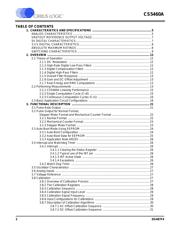
LIST OF FIGURES
Figure 1. CS5460A Read and Write Timing Diagrams..................................................................10
Figure 2. CS5460A Auto-Boot Sequence Timing..........................................................................11
Figure 3. Data Flow.......................................................................................................................13
Figure 4. Voltage Input Filter Characteristics................................................................................14
Figure 5. Current Input Filter Characteristics ................................................................................14
Figure 6. Typical Connection Diagram (One-Phase 2-Wire, Direct Connect to Power Line)........17
Figure 7. Typical Connection Diagram (One-Phase 2-Wire, Isolated from Power Line)...............18
Figure 8. Typical Connection Diagram (One-Phase 3-Wire).........................................................19
Figure 9. Typical Connection Diagram (One-Phase 3-Wire - No Neutral Available).....................20
Figure 10. Time-plot representation of pulse output for a typical burst of pulses (Normal Format)23
Figure 11. Mechanical Counter Format on EOUT and EDIR ........................................................23
Figure 12. Stepper Motor Format on EOUT and EDIR .................................................................24
Figure 13. Typical Interface of EEPROM to CS5460A..................................................................24
Figure 14. Timing Diagram for Auto-Boot Sequence ....................................................................25
Figure 15. Oscillator Connection...................................................................................................27
Figure 16. System Calibration of Gain. .........................................................................................30
Figure 17. System Calibration of Offset. .......................................................................................30
Figure 18. Calibration Data Flow...................................................................................................30
Figure 19. Example of AC Gain Calibration ..................................................................................31
Figure 20. Input Protection for Single-Ended Input Configurations...............................................37
Figure 21. CS5460A Register Diagram.........................................................................................44
LIST OF TABLES
Table 1. Differential Input Voltage vs. Output Code......................................................................14
Table 2. Available range of ±0.1% output linearity,
with default settings in the gain/offset registers. ...........................................................15
Table 3. Default Register Values upon Reset Event.....................................................................43
器件 Datasheet 文档搜索
AiEMA 数据库涵盖高达 72,405,303 个元件的数据手册,每天更新 5,000 多个 PDF 文件
