Datasheet 搜索 > MOS管 > TI(德州仪器) > CSD25484F4 数据手册 > CSD25484F4 其他数据使用手册 5/26 页

¥ 0.104
CSD25484F4 其他数据使用手册 - TI(德州仪器)
制造商:
TI(德州仪器)
分类:
MOS管
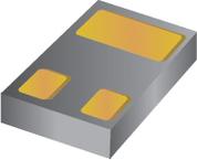
封装:
PICOSTAR-3
描述:
CSD25484F4 20V P 通道 FemtoFET™ MOSFET
Pictures:
3D模型
符号图
焊盘图
引脚图
产品图
页面导航:
导航目录
CSD25484F4数据手册
Page:
of 26 Go
若手册格式错乱,请下载阅览PDF原文件
0
5
10
15
20
0 10 20 30 40 50 60 70 80 90
Ambient Temperature (ºC)
Output Current (A)
400LFM
200LFM
100LFM
Nat Conv
G001
0
5
10
15
20
0 20 40 60 80 100 120 140
Board Temperature (ºC)
Output Current (A)
V
IN
= 12V
V
GS
= 5V
V
OUT
= 1.3V
f
SW
= 500kHz
L
OUT
= 0.95µH
G001
0
0.5
1
1.5
2
2.5
3
3.5
4
4.5
5
1 2 3 4 5 6 7 8 9 10 11 12 13 14 15
Output Current (A)
Power Loss (W)
V
IN
= 12V
V
GS
= 5V
V
OUT
= 1.3V
f
SW
= 500kHz
L
OUT
= 0.95µH
G001
0.5
0.6
0.7
0.8
0.9
1
1.1
−50 −25 0 25 50 75 100 125 150
Junction Temperature (ºC)
Power Loss, Normalized
V
IN
= 12V
V
GS
= 5V
V
OUT
= 1.3V
f
SW
= 500kHz
L
OUT
= 0.95µH
G001
CSD87381P
www.ti.com.cn
ZHCSAY2F –MARCH 2013–REVISED MARCH 2015
Max R
θJA
= 84°C/W Max R
θJA
= 184°C/W
when mounted on when mounted on
1 inch
2
(6.45 cm
2
) of minimum pad area of 2
2 oz. (0.071 mm thick) oz. (0.071 mm thick)
Cu. Cu.
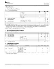
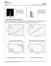
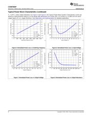
5.6 Typical Power Block Characteristics
T
J
= 125°C, unless stated otherwise. For Figure 3 and Figure 4, the Typical Power Block System Characteristic curves are
based on measurements made on a PCB design with dimensions of 4 inches (W) × 3.5 inches (L) × 0.062 inch (H) and 6
copper layers of 1 oz. copper thickness. See Application and Implementation for detailed explanation.
Figure 1. Power Loss vs Output Current Figure 2. Normalized Power Loss vs Temperature
Figure 3. Safe Operating Area – PCB Horizontal Mount Figure 4. Typical Safe Operating Area
Copyright © 2013–2015, Texas Instruments Incorporated 5
器件 Datasheet 文档搜索
AiEMA 数据库涵盖高达 72,405,303 个元件的数据手册,每天更新 5,000 多个 PDF 文件
