Datasheet 搜索 > FPGA芯片 > Altera(阿尔特拉) > EP2C20F484C8 数据手册 > EP2C20F484C8 产品封装文件 5/470 页
 器件3D模型
¥ 439.757
EP2C20F484C8 产品封装文件 - Altera(阿尔特拉)
制造商:
Altera(阿尔特拉)
分类:
FPGA芯片
封装:
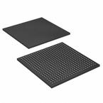
FBGA-484
描述:
FPGA - 现场可编程门阵列 FPGA - Cyclone II 1172 LABs 315 IOs
Pictures:
3D模型
符号图
焊盘图
引脚图
产品图
页面导航:
引脚图在P190P411P428Hot
典型应用电路图在P28P30P32
原理图在P28P100P189P217P229P259
封装尺寸在P12P449P451P452P453P454P455P456P457P458P459P460
型号编码规则在P11P181P453P455P457P459P461P463P465P467
功能描述在P27
技术参数、封装参数在P11P77P92P97P98P100P105P107P109P111P113P115
应用领域在P119P120P121P122P181P331P333P445
电气规格在P298P319P329P331P333


导航目录
EP2C20F484C8数据手册
Page:
of 470 Go
若手册格式错乱,请下载阅览PDF原文件

Altera Corporation v
Cyclone II Device Handbook, Volume 1
Contents
Internal Timing ............................................................................................................................... 5–18
Cyclone II Clock Timing Parameters ........................................................................................... 5–23
Clock Network Skew Adders .......................................................................................................5–29
IOE Programmable Delay ............................................................................................................. 5–30
Default Capacitive Loading of Different I/O Standards .......................................................... 5–31
I/O Delays ....................................................................................................................................... 5–33
Maximum Input and Output Clock Rate .................................................................................... 5–46
High Speed I/O Timing Specifications ....................................................................................... 5–55
External Memory Interface Specifications .................................................................................. 5–63
JTAG Timing Specifications .......................................................................................................... 5–64
PLL Timing Specifications ............................................................................................................ 5–66
Duty Cycle Distortion ......................................................................................................................... 5–67
DCD Measurement Techniques ................................................................................................... 5–68
Referenced Documents ....................................................................................................................... 5–74
Document Revision History ............................................................................................................... 5–74
Chapter 6. Reference & Ordering Information
Software .................................................................................................................................................. 6–1
Device Pin-Outs ..................................................................................................................................... 6–1
Ordering Information ........................................................................................................................... 6–1
Document Revision History ................................................................................................................. 6–2
Section II. Clock Management
Revision History .................................................................................................................................... 6–1
Chapter 7. PLLs in Cyclone II Devices
Introduction ............................................................................................................................................ 7–1
Cyclone II PLL Hardware Overview .................................................................................................. 7–2
PLL Reference Clock Generation ................................................................................................... 7–6
Clock Feedback Modes ....................................................................................................................... 7–10
Normal Mode .................................................................................................................................. 7–10
Zero Delay Buffer Mode ................................................................................................................ 7–11
No Compensation Mode ............................................................................................................... 7–12
Source-Synchronous Mode ........................................................................................................... 7–13
Hardware Features .............................................................................................................................. 7–14
Clock Multiplication & Division .................................................................................................. 7–14
Programmable Duty Cycle ........................................................................................................... 7–15
Phase-Shifting Implementation .................................................................................................... 7–16
Control Signals ................................................................................................................................ 7–17
Manual Clock Switchover ............................................................................................................. 7–20
Clocking ................................................................................................................................................ 7–21
Global Clock Network ................................................................................................................... 7–21
Clock Control Block ....................................................................................................................... 7–24
Global Clock Network Clock Source Generation ...................................................................... 7–26
Global Clock Network Power Down ........................................................................................... 7–28
器件 Datasheet 文档搜索
AiEMA 数据库涵盖高达 72,405,303 个元件的数据手册,每天更新 5,000 多个 PDF 文件
