Datasheet 搜索 > FPGA芯片 > Altera(阿尔特拉) > EP2C20F484C8 数据手册 > EP2C20F484C8 产品封装文件 6/470 页
 器件3D模型
¥ 439.72
EP2C20F484C8 产品封装文件 - Altera(阿尔特拉)
制造商:
Altera(阿尔特拉)
分类:
FPGA芯片
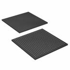
封装:
FBGA-484
描述:
FPGA - 现场可编程门阵列 FPGA - Cyclone II 1172 LABs 315 IOs
Pictures:
3D模型
符号图
焊盘图
引脚图
产品图
页面导航:
引脚图在P190P411P428Hot
典型应用电路图在P28P30P32
原理图在P28P100P189P217P229P259
封装尺寸在P12P449P451P452P453P454P455P456P457P458P459P460
型号编码规则在P11P181P453P455P457P459P461P463P465P467
功能描述在P27
技术参数、封装参数在P11P77P92P97P98P100P105P107P109P111P113P115
应用领域在P119P120P121P122P181P331P333P445
电气规格在P298P319P329P331P333


导航目录
EP2C20F484C8数据手册
Page:
of 470 Go
若手册格式错乱,请下载阅览PDF原文件

vi Altera Corporation
Cyclone II Device Handbook, Volume 1
Contents
clkena signals .................................................................................................................................. 7–29
Board Layout ........................................................................................................................................ 7–30
VCCA & GNDA ............................................................................................................................. 7–31
VCCD & GND ................................................................................................................................. 7–33
Conclusion ............................................................................................................................................ 7–33
Section III. Memory
Revision History .................................................................................................................................... 7–1
Chapter 8. Cyclone II Memory Blocks
Introduction ............................................................................................................................................ 8–1
Overview ................................................................................................................................................. 8–1
Control Signals .................................................................................................................................. 8–3
Parity Bit Support ............................................................................................................................. 8–4
Byte Enable Support ........................................................................................................................ 8–4
Packed Mode Support ..................................................................................................................... 8–6
Address Clock Enable ...................................................................................................................... 8–6
Memory Modes ...................................................................................................................................... 8–8
Single-Port Mode .............................................................................................................................. 8–9
Simple Dual-Port Mode ................................................................................................................. 8–10
True Dual-Port Mode ..................................................................................................................... 8–12
Shift Register Mode ........................................................................................................................ 8–14
ROM Mode ...................................................................................................................................... 8–16
FIFO Buffer Mode ........................................................................................................................... 8–16
Clock Modes ......................................................................................................................................... 8–16
Independent Clock Mode .............................................................................................................. 8–17
Input/Output Clock Mode ........................................................................................................... 8–19
Read/Write Clock Mode ............................................................................................................... 8–22
Single-Clock Mode ......................................................................................................................... 8–24
Power-Up Conditions & Memory Initialization ........................................................................ 8–27
Read-During- Write Operation at the Same Address .................................................................... 8–28
Same-Port Read-During-Write Mode .......................................................................................... 8–28
Mixed-Port Read-During-Write Mode ........................................................................................ 8–29
Conclusion ............................................................................................................................................ 8–30
Referenced Documents ....................................................................................................................... 8–30
Chapter 9. External Memory Interfaces
Introduction ............................................................................................................................................ 9–1
External Memory Interface Standards ................................................................................................ 9–2
DDR & DDR2 SDRAM .................................................................................................................... 9–2
QDRII SRAM ..................................................................................................................................... 9–5
Cyclone II DDR Memory Support Overview .................................................................................... 9–9
Data & Data Strobe Pins ................................................................................................................ 9–10
Clock, Command & Address Pins ............................................................................................... 9–14
Parity, DM & ECC Pins ................................................................................................................. 9–14
器件 Datasheet 文档搜索
AiEMA 数据库涵盖高达 72,405,303 个元件的数据手册,每天更新 5,000 多个 PDF 文件
