Datasheet 搜索 > MOS管 > Fairchild(飞兆/仙童) > FDC6333C 数据手册 > FDC6333C 其他数据使用手册 2/10 页

¥ 1.999
FDC6333C 其他数据使用手册 - Fairchild(飞兆/仙童)
制造商:
Fairchild(飞兆/仙童)
分类:
MOS管
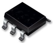
封装:
TSOT-23-6
描述:
FAIRCHILD SEMICONDUCTOR FDC6333C 双路场效应管, MOSFET, N和P沟道, 2.5 A, 30 V, 0.095 ohm, 10 V, 1.8 V
Pictures:
3D模型
符号图
焊盘图
引脚图
产品图
页面导航:

导航目录
FDC6333C数据手册
Page:
of 10 Go
若手册格式错乱,请下载阅览PDF原文件
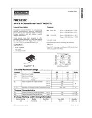
October 2001
2001 Fairchild Semiconductor Corporation
FDC6333C Rev C (W)
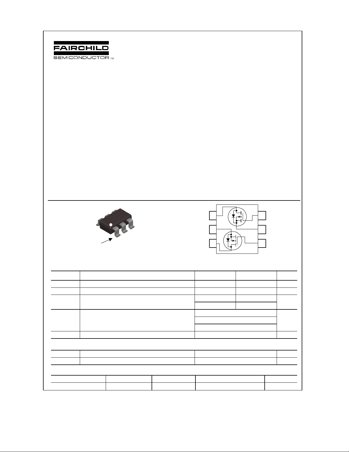
FDC6333C
30V N & P-Channel PowerTrench
MOSFETs
General Description
These N & P-Channel MOSFETs are produced using
Fairchild Semiconductor’s advanced PowerTrench
process that has been especially tailored to minimize
on-state resistance and yet maintain superior
switching performance.
These devices have been designed to offer
exceptional power dissipation in a very small footprint
for applications where the bigger more expensive
SO-8 and TSSOP-8 packages are impractical.
Applications
• DC/DC converter
• Load switch
• LCD display inverter
Features
• Q1 2.5 A, 30V. R
DS(ON)
= 95 mΩ @ V
GS
= 10 V
R
DS(ON)
= 150 mΩ @ V
GS
= 4.5 V
• Q2 –2.0 A, 30V. R
DS(ON)
= 150 mΩ @ V
GS
= –10 V
R
DS(ON)
= 220 mΩ @ V
GS
= –4.5 V
• Low gate charge
• High performance trench technology for extremely
low R
DS(ON)
.
• SuperSOT –6 package: small footprint (72% smaller than
SO-8); low profile (1mm thick).
D1
S2
G1
D2
S1
G2
SuperSOT -6
TM
Pin 1
SuperSOT™-6
3
2
1
4
5
6
Q1(N)
Q2(P)
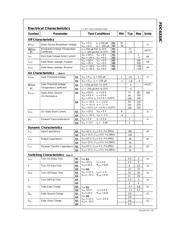
Absolute Maximum Ratings T
A
=25
o
C unless otherwise noted
Symbol Parameter Q1 Q2 Units
V
DSS
Drain-Source Voltage 30 –30 V
V
GSS
Gate-Source Voltage ±16 ±25 V
I
D
Drain Current – Continuous (Note 1a) 2.5 –2.0 A
– Pulsed 8 –8
Power Dissipation for Single Operation (Note 1a) 0.96
(Note 1b)
0.9
P
D
(Note 1c)
0.7
W
T
J
, T
STG
Operating and Storage Junction Temperature Range –55 to +150
°C
Thermal Characteristics
R
θJA
Thermal Resistance, Junction-to-Ambient (Note 1a) 130
°C/W
R
θJC
Thermal Resistance, Junction-to-Case (Note 1) 60
°C/W
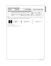
Package Marking and Ordering Information
Device Marking Device Reel Size Tape width Quantity
.333 FDC6333C 7’’ 8mm 3000 units
FDC6333C
器件 Datasheet 文档搜索
AiEMA 数据库涵盖高达 72,405,303 个元件的数据手册,每天更新 5,000 多个 PDF 文件
