Datasheet 搜索 > 光耦合器/光隔离器 > Vishay Semiconductor(威世) > H11B1 数据手册 > H11B1 其他数据使用手册 2/6 页
 器件3D模型
¥ 3.646
H11B1 其他数据使用手册 - Vishay Semiconductor(威世)
制造商:
Vishay Semiconductor(威世)
分类:
光耦合器/光隔离器
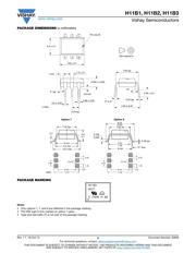
封装:
DIP-6
描述:
H11B1 系列 单通道 5300 Vrms 500 % CTR 光电晶体管 光耦合器-DIP-6
Pictures:
3D模型
符号图
焊盘图
引脚图
产品图
页面导航:

导航目录
H11B1数据手册
Page:
of 6 Go
若手册格式错乱,请下载阅览PDF原文件
H11B1, H11B2, H11B3
www.vishay.com
Vishay Semiconductors
Rev. 1.7, 19-Oct-12
2
Document Number: 83609
For technical questions, contact: optocoupleranswers@vishay.com
THIS DOCUMENT IS SUBJECT TO CHANGE WITHOUT NOTICE. THE PRODUCTS DESCRIBED HEREIN AND THIS DOCUMENT
ARE SUBJECT TO SPECIFIC DISCLAIMERS, SET FORTH AT www.vishay.com/doc?91000
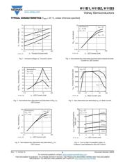
Note
• Stresses in excess of the absolute maximum ratings can cause permanent damage to the device. Functional operation of the device is not
implied at these or any other conditions in excess of those given in the operational sections of this document. Exposure to absolute
maximum ratings for extended periods of the time can adversely affect reliability.
Note
• Minimum and maximum values were tested requierements. Typical values are characteristics of the device and are the result of engineering
evaluations. Typical values are for information only and are not part of the testing requirements.
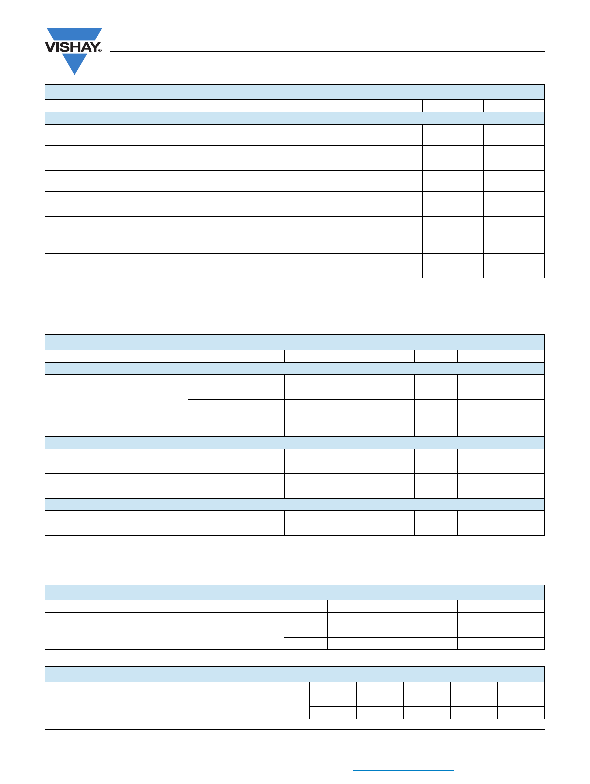
COUPLER
Isolation test voltage
between emitter and detector
V
ISO
5300 V
RMS
Creepage distance ≥ 7mm
Clearance distance ≥ 7mm
Comparative tracking index per
DIN IEC 112/VDE 0303, part 1
CTI 175
Isolation resistance
V
IO
= 500 V, T
amb
= 25 °C R
IO
≥ 10
12
Ω
V
IO
= 500 V, T
amb
= 100 °C R
IO
≥ 10
11
Ω
Total package dissipation (LED plus detector) P
tot
260 mW
Derate linearly from 25 °C 3.5 mW/°C
Storage temperature T
stg
- 55 to + 150 °C
Operating temperature T
amb
- 55 to + 100 °C
Lead soldering time at 260 °C 10 s
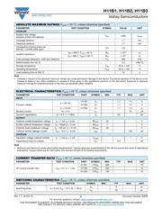
ELECTRICAL CHARACTERISTICS (T
amb
= 25 °C, unless otherwise specified)
PARAMETER TEST CONDITION PART SYMBOL MIN. TYP. MAX. UNIT
INPUT
Forward voltage
I
F
= 50 mA
H11B1 V
F
1.1 1.5 V
H11B2 V
F
1.1 1.5 V
I
F
= 10 mA H11B3 V
F
1.1 1.5 V
Reverse current V
R
= 3 V I
R
10 μA
Junction capacitance V
F
= 0 V, f = 1 MHz C
j
50 pF
OUTPUT
Collector emitter breakdown voltage I
C
= 1 mA, I
F
= 0 mA BV
CEO
30 V
Emitter collector breakdown voltage I
E
= 100μA, I
F
= 0 mA BV
ECO
7V
Collector base breakdown voltage I
C
= 100 μA , I
F
= 0 mA BV
CBO
30 V
Collector emitter leakage current V
CE
= 10 V, I
F
= 0 mA I
CEO
100 nA
COUPLER
Saturation voltage collector-emitter I
F
= 1 mA, I
C
= 1 mA V
CEsat
1V
Capacitance (input to output) C
IO
0.5 pF
CURRENT TRANSFER RATIO (T
amb
= 25 °C, unless otherwise specified)
PARAMETER TEST CONDITION PART SYMBOL MIN. TYP. MAX. UNIT
DC current transfer ratio V
CE
= 5 V, I
F
= 1 mA
H11B1 CTR
DC
500 %
H11B2 CTR
DC
200 %
H11B3 CTR
DC
100 %
SWITCHING CHARACTERISTICS (T
amb
= 25 °C, unless otherwise specified)
PARAMETER TEST CONDITION SYMBOL MIN. TYP. MAX. UNIT
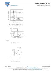
Switching times I
F
= 5 mA, V
CE
= 10 V, R
L
= 100 Ω
t
on
5μs
t
off
30 μs
ABSOLUTE MAXIMUM RATINGS (T
amb
= 25 °C, unless otherwise specified)
PARAMETER TEST CONDITION SYMBOL VALUE UNIT
器件 Datasheet 文档搜索
AiEMA 数据库涵盖高达 72,405,303 个元件的数据手册,每天更新 5,000 多个 PDF 文件
